Hello! Welcome to the next lesson in our journey through radioelectronics.
In our last lesson, we explored the fascinating physics of the P-N junction at thermal equilibrium, understanding how a built-in potential barrier naturally forms. Today, we'll see what happens when we intentionally disturb that equilibrium by applying an external voltage.
Introduction
Approximate time to complete: 45 minutes
This lesson addresses the learning outcome: Diode Operation: Forward and Reverse Bias Characteristics. We will apply an external voltage, or "bias," to the P-N junction and investigate the two fundamental modes of operation that result. Understanding these characteristics is the key to unlocking the diode's primary function as a one-way gate for electrical current.
By the end of this lesson, you will be able to explain:
- How to apply forward bias and its effect on the depletion region, potential barrier, and current flow.
- How to apply reverse bias and its effect on the depletion region, potential barrier, and current flow.
- The origin and behavior of the small reverse saturation current.
- How to interpret the diode's current-voltage (I-V) characteristic curve.
We'll build directly on our model of the P-N junction, moving from a static equilibrium state to a dynamic, controlled one.
1. The Diode: A One-Way Valve for Current
Before diving into the semiconductor physics, let's start with a high-level analogy. A diode's primary role in a circuit is to allow current to flow easily in one direction but block it from flowing in the opposite direction.
Please watch the first minute of this video, which introduces this core concept using a simple water pipe analogy.
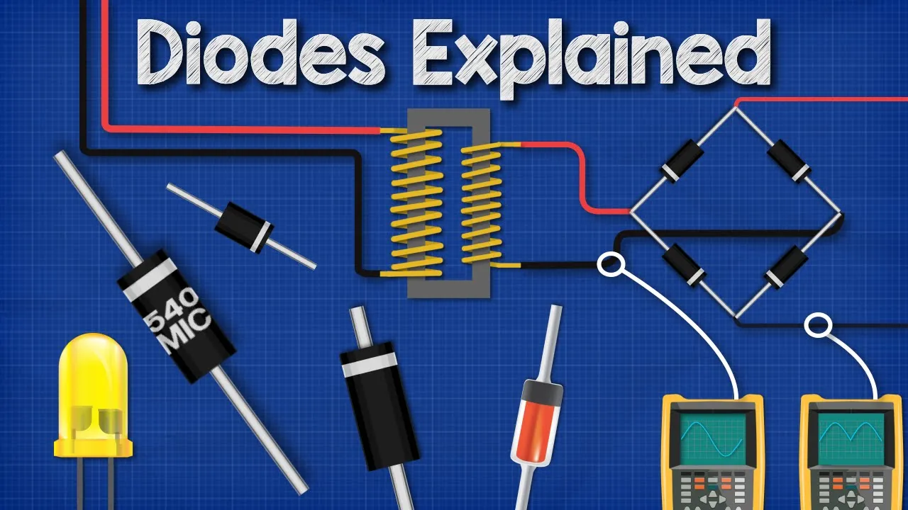
- What to focus on: The video compares a diode to a one-way swing valve in a pipe. This simple mechanical analogy perfectly captures the diode's essential function.
- Time: 00:04 - 01:14
As you saw, the diode has two terminals:
- Anode: The P-type side.
- Cathode: The N-type side (often marked with a stripe on the component's body).
The two modes of operation, which depend on the polarity of the voltage we apply, are called forward bias and reverse bias.
2. Forward Bias: Opening the Gate
To forward bias a diode, we connect the positive terminal of a voltage source to the P-side (anode) and the negative terminal to the N-side (cathode).
This applied external electric field opposes the junction's internal built-in electric field. Think of it as pushing against the natural barrier we discussed in the last lesson.
The consequences are profound:
- Barrier Lowering: The net potential barrier across the junction is reduced from to .
- Depletion Region Narrowing: The positive terminal repels holes from the P-side, and the negative terminal repels electrons from the N-side, pushing them towards the junction. This neutralizes some of the fixed ions and shrinks the depletion region.
- Current Flow: Once the applied voltage is large enough to significantly lower the barrier (for silicon, this is around 0.7 V), majority carriers have enough energy to diffuse across the junction in large numbers. Electrons from the N-side cross to the P-side, and holes from the P-side cross to the N-side. This large flow of majority carriers constitutes the forward current.
The following video provides an excellent animated explanation of this entire process.
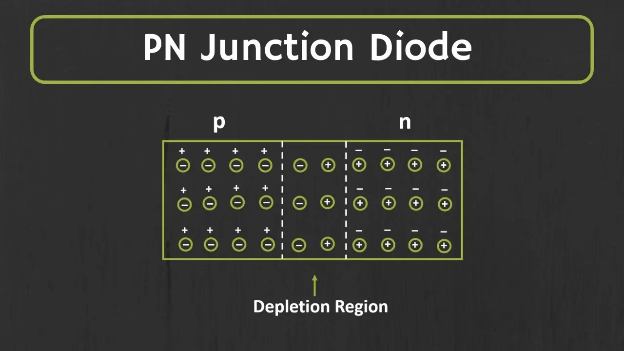
- What to focus on: Observe how the applied voltage pushes the majority carriers toward the junction, causing the depletion region to shrink. See how this allows a significant current to flow once the barrier is overcome.
- Time: 06:48 - 09:51
In summary, forward bias effectively "turns on" the diode, allowing it to conduct current with very little resistance.
3. Reverse Bias: Closing the Gate
To reverse bias a diode, we do the opposite: connect the negative terminal of the voltage source to the P-side (anode) and the positive terminal to the N-side (cathode).
This applied external field now aids the junction's internal built-in field, reinforcing the barrier.
The effects are the mirror image of forward bias:
- Barrier Raising: The net potential barrier across the junction increases to .
- Depletion Region Widening: The negative terminal attracts holes away from the junction on the P-side, while the positive terminal attracts electrons away from the junction on the N-side. This uncovers more fixed ions and expands the depletion region.
- Current Blockage: With such a high potential barrier and wide depletion region, the flow of majority carriers across the junction is effectively blocked.
So, does any current flow? Yes, but it's a tiny amount due to a different mechanism. Recall that both P-type and N-type materials have a small number of minority carriers. The strong electric field across the widened depletion region sweeps these minority carriers across the junction. This constitutes a very small current called the reverse saturation current ().
This current is called "saturation" because its magnitude depends on the number of available minority carriers, not on the applied reverse voltage. Since minority carriers are generated by thermal energy, is highly dependent on temperature.
The same video explains this beautifully.
- What to focus on: Watch how the charge carriers are pulled away from the junction, widening the depletion region. Pay close attention to the explanation of how minority carriers are responsible for the small reverse saturation current and its dependence on temperature.
- Time: 09:51 - 13:00
In reverse bias, the diode is effectively "off," acting as an insulator that blocks significant current flow.
4. The I-V Characteristic Curve
We can summarize the diode's behavior by plotting its current () versus the voltage across it (). This is the fundamental I-V characteristic curve.
- What to focus on: This segment introduces the shape of the I-V curve, visually connecting the concepts of forward and reverse bias.
- Time: 07:16 - 08:00
Let's break down the curve based on what we've learned:
-
First Quadrant (Forward Bias, ):
- For small positive voltages (less than the "turn-on" or "knee" voltage, ~0.7V for silicon), the current is almost zero. The barrier is lowered but not enough for significant diffusion.
- As the voltage crosses this threshold, the current begins to increase exponentially. A small increase in voltage leads to a large increase in current.
-
Third Quadrant (Reverse Bias, ):
- As the reverse voltage increases, a very small, almost constant negative current flows. This is the reverse saturation current, . For modern silicon diodes, this is typically in the nanoampere (nA) to microampere (μA) range.
-
Breakdown Region (not shown in detail):
- If the reverse voltage becomes excessively large (e.g., -50V, -100V), the diode will enter reverse breakdown and a large current will flow. This is usually destructive, but it is the operating principle of a special type called the Zener diode, which we will cover in a later lesson.
The I-V curve is the diode's fingerprint, encapsulating its non-linear, one-way conducting behavior in a single graph.
Conclusion
In this lesson, we moved from the static equilibrium of the P-N junction to its dynamic operation under an external voltage.
Let's summarize the key takeaways:
- Forward Bias: Connects P-type to positive and N-type to negative. It lowers the potential barrier, narrows the depletion region, and allows a large current of majority carriers to flow. The diode is ON.
- Reverse Bias: Connects P-type to negative and N-type to positive. It raises the potential barrier, widens the depletion region, and blocks majority carriers. A tiny reverse saturation current of minority carriers flows. The diode is OFF.
- I-V Curve: This graph visually represents the diode's behavior, showing an exponential current increase in forward bias and a near-zero current in reverse bias, confirming its role as a one-way electrical valve.
You now have a solid qualitative understanding of how a diode functions. This is the most crucial conceptual step in this module.
Preview of the Next Lesson:
Our discussion today has been descriptive. How can we model this behavior mathematically? In the next lesson, The Diode Equation: Modeling the I-V Relationship, we will introduce the Shockley diode equation, a powerful formula that precisely describes the I-V curve and allows us to perform quantitative circuit analysis.