Hello! Welcome back to our course on Radioelectronics. In the previous lesson, we established a solid foundation by reviewing how semiconductors are doped to create P-type and N-type materials. Now, we'll explore the fascinating and crucial phenomena that occur when these two types of materials are brought together.
Introduction
Approximate time to complete: 40 minutes
This lesson addresses the second learning outcome of the "Semiconductor Physics and Diode Circuits" module: The P-N Junction: Formation of the Depletion Region and Built-in Potential. We will investigate the physical processes that occur at the interface between P-type and N-type silicon, which spontaneously create a structure with profound electrical properties. This P-N junction is the fundamental building block of diodes, transistors, and nearly all modern semiconductor devices.
By the end of this lesson, you will be able to explain:
- The roles of diffusion and drift currents in the formation of the junction.
- How the depletion region is formed and what it consists of.
- The origin of the built-in electric field and the corresponding built-in potential ().
- How to represent the P-N junction at equilibrium using an energy band diagram.
We will focus entirely on the junction at thermal equilibrium, meaning with no external voltage applied. This state is the baseline from which all diode behavior originates.
1. Physical Formation of the P-N Junction
Let's imagine bringing a block of P-type silicon into perfect contact with a block of N-type silicon. While fabrication is more complex, this model helps us understand the physics.
- The N-type region has a high concentration of free electrons (majority carriers).
- The P-type region has a high concentration of holes (majority carriers).
This large concentration gradient at the junction drives a powerful physical process: diffusion.
Diffusion and Recombination
Just as a drop of ink spreads out in water, the free electrons from the N-side begin to diffuse across the junction into the P-side. Similarly, holes from the P-side diffuse into the N-side.
When a free electron from the N-side crosses into the P-side, it soon encounters a hole and recombines. The free electron fills the vacancy, and in doing so, both the free electron and the hole cease to exist as mobile charge carriers.
This process has a critical consequence.
- When the N-region loses an electron, the donor atom it left behind is no longer electrically neutral. It now has a net positive charge (it's an ionized donor).
- When the P-region loses a hole (by an electron filling it), the acceptor atom becomes negatively charged (an ionized acceptor).
These ionized atoms are fixed in the crystal lattice; they cannot move. As diffusion and recombination continue, a region on both sides of the junction becomes populated by these fixed, charged ions and is stripped of mobile carriers. This area is aptly named the depletion region.
To visualize this process, please watch the following segment.
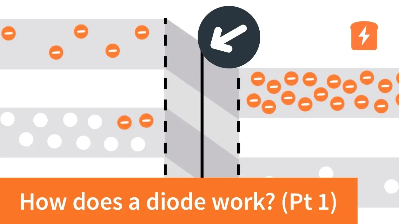
Focus on the animated depiction of electron and hole diffusion, their recombination, and the resulting layers of fixed positive and negative charges that form the depletion region. (00:43 - 01:46)
2. The Built-in Electric Field and Potential
The depletion region now consists of a layer of fixed positive ions on the N-side and a layer of fixed negative ions on the P-side. This separation of charge, known as a space charge region, creates an electric field () that points from the positive N-side to the negative P-side.
This electric field exerts a force on any mobile charge carriers.
- It pushes any free electrons near the junction back toward the N-side.
- It pushes any holes near the junction back toward the P-side.
This movement of carriers due to the electric field is a drift current. This drift current is in the opposite direction to the diffusion current.
Initially, the diffusion current is strong. But as the depletion region grows, the electric field becomes stronger, and so does the opposing drift current. The system quickly reaches thermal equilibrium when the magnitude of the diffusion current is perfectly balanced by the magnitude of the drift current. At this point, there is no net flow of charge across the junction.
The electric field across the depletion region creates a potential difference. This is the built-in potential, often denoted as or barrier potential. It represents the potential barrier that majority carriers must overcome to diffuse across the junction.
Watch the next part of the video for a concise explanation of this field and potential.
Focus on how the charge layers create an electric field and how this gives rise to the barrier potential. (01:46 - 02:23)
At equilibrium, this built-in potential barrier is what holds the diffusion process in check, maintaining a stable depletion region. For silicon at room temperature, is typically around 0.6 to 0.7 volts.
3. The Energy Band Diagram at Equilibrium
A more formal and powerful way to understand the P-N junction is through its energy band diagram. Your background in radiophysics makes this perspective particularly valuable.
Recall from the last lesson:
- In P-type material, the Fermi level () is close to the valence band ().
- In N-type material, the Fermi level () is close to the conduction band ().
When the two materials are joined and reach thermal equilibrium, a fundamental rule of thermodynamics applies: the Fermi energy level, , must be constant throughout the entire system. If it weren't, electrons would flow to a region of lower energy, which means the system wouldn't be in equilibrium.
The following video introduces this crucial principle.
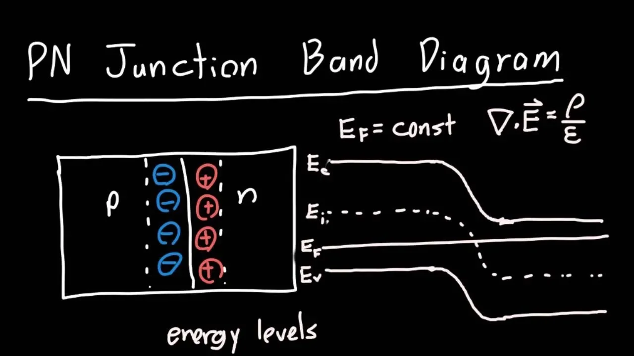
Watch this short segment to understand why the Fermi level must be constant. (02:59 - 03:59)
To align the different Fermi levels of the isolated P-type and N-type materials into a single, constant level, the energy bands must bend in the vicinity of the junction. The N-side bands move down, and the P-side bands move up, until their Fermi levels align.
This "bending" of the bands creates an energy hill, or potential barrier, that an electron from the N-side conduction band must climb to get to the P-side conduction band. The height of this hill is the built-in potential in energy units ().
The next segment of the video masterfully illustrates how to construct this diagram and derives the mathematical expression for the built-in potential.
Watch how the individual band diagrams are connected and pay close attention to the derivation of the built-in potential equation. (03:42 - 07:29)
The built-in potential is the difference between the intrinsic Fermi levels () on the P and N sides, divided by the elementary charge . As derived in the video, this leads to the fundamental equation for the built-in potential:
Where:
- is the Boltzmann constant ( J/K)
- is the absolute temperature in Kelvin
- is the elementary charge ( C)
- is the concentration of acceptor atoms in the P-type material
- is the concentration of donor atoms in the N-type material
- is the intrinsic carrier concentration of the semiconductor (for silicon, cm⁻³ at room temperature)
The term is often called the thermal voltage, , which is approximately 26 mV at room temperature (300 K).
This equation elegantly shows that the built-in potential is not a fixed constant but depends on the doping levels and temperature—a cornerstone concept in device physics.
For another excellent animated view of this band-bending process, you can refer back to the first video we watched.
This section provides a complementary animated visualization of the energy bands aligning. (02:23 - 04:21)
Conclusion
In this lesson, we have dissected the formation of the P-N junction at thermal equilibrium. Let's summarize the key points:
- Diffusion & Depletion: A concentration gradient causes majority carriers to diffuse across the junction and recombine, leaving behind a depletion region of fixed, ionized atoms.
- Equilibrium: An internal electric field forms in the depletion region, creating a drift current that opposes the diffusion current. Equilibrium is reached when these two currents are equal and opposite.
- Built-in Potential: The electric field creates a built-in potential barrier () that prevents further net diffusion. Its value depends on doping concentrations and temperature.
- Energy Bands: At equilibrium, the Fermi level is constant, causing the energy bands to bend at the junction, visually representing the potential barrier.
You now have a clear model of the P-N junction in its resting state. This is the foundation upon which we will build our understanding of how diodes actually work.
Preview of the Next Lesson:
What happens if we disturb this equilibrium? In our next lesson, Diode Operation: Forward and Reverse Bias Characteristics, we will apply an external voltage to the P-N junction. We'll see how this external voltage either lowers or raises the potential barrier, leading to the diode's signature one-way conduction of current.