
Hello! In our previous lesson, we established a clear picture of how individual N-channel and P-channel MOSFETs function as efficient, voltage-controlled switches. We saw that an N-channel MOSFET is excellent at creating a path to ground (a "pull-down" switch), while a P-channel MOSFET excels at creating a path to the positive voltage supply (a "pull-up" switch).
This lesson marks a significant step in your journey to see "how every dot connects." We will now combine these complementary transistors to build the workhorses of the digital world: CMOS NAND and NOR gates. You'll learn how their clever pairing not only implements logic but also gives CMOS technology its signature low-power advantage. By the end of this lesson, you will be able to trace the operation of these fundamental gates at the transistor level, moving from a single switch to a true computational element.
The "Complementary" in CMOS Logic
The name CMOS stands for Complementary Metal-Oxide-Semiconductor. The "complementary" part is key. Instead of using just one type of transistor, CMOS logic pairs an N-channel MOSFET with a P-channel MOSFET. This pairing is designed to solve major problems found in older logic families, such as high power consumption.
Let's start with the simplest possible logic gate: an inverter, or a NOT gate.
The operation is beautifully simple and efficient:
-
When Input is LOW (0V):
- The N-MOSFET is OFF (since ). The path to ground is broken.
- The P-MOSFET is ON (since its gate is low relative to its source at ). The path to is complete.
- The output is pulled HIGH.
-
When Input is HIGH ():
- The N-MOSFET is ON (since ). The path to ground is complete.
- The P-MOSFET is OFF (since its gate is high, at the same potential as its source). The path to is broken.
- The output is pulled LOW.
The following video provides an excellent animated walkthrough of this exact process.
Building logic gates from MOSFET transistors
This segment from EngMicroLectures visually demonstrates how the complementary action of the P-MOS and N-MOS transistors creates the NOT function.
Please watch the section covering the NOT gate. Pay close attention to which transistor is conducting (short circuit) versus non-conducting (open circuit) for each input state.
The critical insight here is that in either stable state (output high or low), one of the transistors is always off. This means there is never a direct path from to ground. This lack of a static current path is what makes CMOS logic incredibly power-efficient, allowing for the integration of billions of gates onto a single chip.
The video below elaborates on this advantage, contrasting the CMOS approach with less efficient designs that use only one type of transistor.
CMOS Logic Gates Explained | Logic Gate Implementation using CMOS logic
The channel ALL ABOUT ELECTRONICS explains why the CMOS configuration is superior to single-transistor-type logic.
Watch the segment from here, which details the construction of the CMOS inverter and highlights its low static power consumption as a key benefit of the pull-up/pull-down design.
Building NAND and NOR Gates
Now that we understand the pull-up/pull-down principle, we can extend it to create multi-input gates like NAND and NOR. The design follows a fascinating rule of duality.
- The pull-down network (PDN), built with N-MOSFETs, implements the gate's primary logic. For example, to get a low output for an AND condition, we connect N-MOSFETs in series.
- The pull-up network (PUN), built with P-MOSFETs, implements the dual of the PDN's logic. If the N-MOSFETs are in series, the corresponding P-MOSFETs will be in parallel.
This structure guarantees that for any valid input combination, either the PUN or the PDN is conducting, but never both at the same time.
[PDF] ECE 410: VLSI Design Course Lecture Notes
These lecture notes from Michigan State University formalize the "push-pull" concept and the rules for constructing CMOS logic gates.
Please read the sections on page 2.10 titled “Push-Pull” Logic and on page 2.11 titled Creating Logic Gates in CMOS. This will give you the formal design principles we are about to apply.
CMOS NAND Gate
A 2-input NAND gate produces a LOW output only when both input A AND input B are HIGH.
- Pull-Down Network (NMOS): To implement the
A AND Blogic, we connect two N-MOSFETs in series. The path to ground is only complete if both transistors are ON. - Pull-Up Network (PMOS): The dual of series is parallel. We connect two P-MOSFETs in parallel. If either A or B is LOW, at least one of the P-MOSFETs will turn ON, creating a path to .
The resulting circuit is shown below.
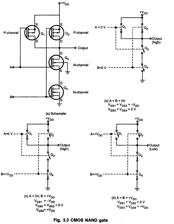
Let's trace its operation using the image above:
- (b) A=0, B=0: Q1 and Q2 are ON, connecting the output to . Q3 and Q4 are OFF. Output is HIGH.
- (c) A=0, B=1: Q1 is ON, connecting the output to . Q3 is OFF, breaking the path to ground. Output is HIGH.
- (Not shown, but symmetrical to c) A=1, B=0: Q2 is ON, connecting the output to . Q4 is OFF, breaking the path to ground. Output is HIGH.
- (d) A=1, B=1: Q1 and Q2 are OFF. Q3 and Q4 are ON, connecting the output to ground. Output is LOW.
This behavior perfectly matches the truth table for a NAND gate. The following video provides a dynamic visualization of this process.
Building logic gates from MOSFET transistors
This animation from EngMicroLectures clearly shows the series N-MOS and parallel P-MOS structure and steps through each combination of inputs for the NAND gate.
Watch the detailed explanation from this segment. Follow how the "open" and "short" circuits form for each case to produce the final output.
CMOS NOR Gate
A 2-input NOR gate produces a LOW output if input A OR input B is HIGH.
- Pull-Down Network (NMOS): To implement the
A OR Blogic, we connect two N-MOSFETs in parallel. The path to ground is complete if either transistor is ON. - Pull-Up Network (PMOS): The dual of parallel is series. We connect two P-MOSFETs in series. The path to is only complete if both transistors are ON (i.e., when both A and B are LOW).
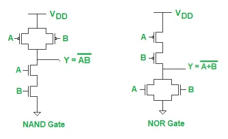
Let's trace the operation of the NOR gate on the right:
- A=0, B=0: Both P-MOSFETs are ON, completing the series path to . Both N-MOSFETs are OFF. Output is HIGH.
- A=0, B=1: The top P-MOSFET is ON, but the bottom one is OFF, breaking the series path to . The N-MOSFET for input B is ON, creating a parallel path to ground. Output is LOW.
- A=1, B=0: The bottom P-MOSFET is ON, but the top one is OFF, breaking the path. The N-MOSFET for input A is ON, creating a path to ground. Output is LOW.
- A=1, B=1: Both P-MOSFETs are OFF. Both N-MOSFETs are ON, creating two paths to ground. Output is LOW.
Once again, the behavior perfectly matches the NOR truth table. The video below provides the corresponding animation.
Building logic gates from MOSFET transistors
This final segment shows the construction and operation of the NOR gate, highlighting the series P-MOS and parallel N-MOS structure.
Watch the NOR gate walkthrough from here. Observe how a HIGH on either input is sufficient to create a path to ground and pull the output low.
Conclusion
In this lesson, you have successfully bridged the gap between individual transistors and functional logic gates. By understanding the complementary "push-pull" design of CMOS, you can now see how all digital logic is built from these simple, repeating patterns.
Here are the key takeaways:
- CMOS logic uses complementary pairs of P-MOSFETs (in a pull-up network) and N-MOSFETs (in a pull-down network).
- This design results in nearly zero static power consumption because there is no direct path between the power supply and ground in a steady state.
- The pull-up and pull-down networks are duals of each other: a series arrangement in one corresponds to a parallel arrangement in the other.
- A NAND gate is built with N-MOSFETs in series and P-MOSFETs in parallel.
- A NOR gate is built with N-MOSFETs in parallel and P-MOSFETs in series.
You now have a foundational understanding of how the most common logic gates are physically realized. In our next lesson, we will zoom out slightly to compare the practical performance characteristics of the CMOS logic family you just learned about with TTL, an older technology. This will help you understand the real-world engineering trade-offs that led to CMOS dominating the world of digital electronics.
Can't find a good explanation? Sign up and we'll make it for you
Sign up