
Hello! In our last lesson, we delved into the transistor-level construction of CMOS NAND and NOR gates, revealing how their complementary "push-pull" design leads to remarkable power efficiency. You saw how P-MOSFETs and N-MOSFETs work in tandem to create logic functions with almost no static power draw.
This lesson takes a step back from the individual gate to the broader "logic family." We will compare the CMOS technology you've just learned about with its historically significant predecessor, Transistor-Transistor Logic (TTL). By the end of this lesson, you will be able to compare the key electrical characteristics—power consumption, speed, and noise margin—that define these families. This comparison is crucial for understanding why CMOS became the dominant technology for everything from microcontrollers to CPUs, and it provides the practical knowledge needed to work with legacy or mixed-technology systems.
The Fundamental Divide: BJT vs. MOSFET
Before we dive into performance metrics, it's essential to understand the core difference in the technology used to build these logic families.
- CMOS, as you know, is built using MOSFETs (Metal-Oxide-Semiconductor Field-Effect Transistors). As we've discussed, these are voltage-controlled devices. A voltage applied to the gate creates an electric field that controls the flow of current, requiring negligible current to maintain a state.
- TTL, on the other hand, is built using BJTs (Bipolar Junction Transistors). These are current-controlled devices. A small current flowing into the "base" terminal is required to switch the transistor on and allow a larger current to flow through it.
This single difference—voltage control versus current control—is the root cause of most of the performance distinctions we are about to explore.
The following video from the Blueprint IoT channel provides an excellent overview of what TTL and CMOS are and how this fundamental transistor difference impacts their behavior.
What is TTL & CMOS? | TTL vs CMOS explained | TTL CMOS compatibility
This video introduces the concepts of TTL and CMOS, including their historical context, and clearly explains the difference between the BJT and MOSFET technologies they are based on.
Please watch the first two segments. The first, from the beginning, explains the naming and history of TTL. The second segment, from here, explains the structure of CMOS and introduces the critical concepts of current-driven (BJT) vs. voltage-driven (MOSFET) operation and rail-to-rail outputs.
1. Power Consumption
The most dramatic difference between the two families is their power consumption.
Static vs. Dynamic Power
TTL gates have a relatively high static power consumption. Because they are built with current-controlled BJTs, there is always a small amount of current flowing through the internal biasing resistors, even when the logic state is not changing.
CMOS gates have almost zero static power consumption. In a stable state (high or low), one of the complementary MOSFETs in the pull-up/pull-down pair is always off, breaking the path from the power supply () to ground (). The only current that flows is minuscule leakage current.
However, CMOS power consumption is dominated by dynamic power, which is the power used during switching. Each time the output of a CMOS gate changes state, it must charge or discharge the capacitance of its own internal nodes and the inputs of any gates it is connected to. This flow of current to charge/discharge these capacitances consumes power. Dynamic power is described by the formula:
where:
- is the total load capacitance.
- is the supply voltage.
- is the switching frequency.
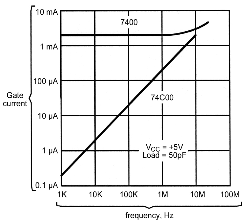
This means CMOS power consumption increases linearly with frequency. At very low frequencies, CMOS is vastly more efficient than TTL. As the frequency rises into the hundreds of MHz, the dynamic power of CMOS can approach and even exceed the static power of TTL.
This relationship is perfectly illustrated in the graph below, which compares the current draw of a classic TTL NAND gate (7400) and a CMOS NAND gate (74C00).
The following reading provides specific values and further explanation of this crucial difference.
TTL vs CMOS Logic: Complete Comparison Guide - PCBSync
This article from PCBSync provides a clear, data-driven comparison of the two logic families.
First, please read the section titled Power Consumption Comparison. Pay close attention to the table comparing static and dynamic power at different frequencies. Then, jump to the FAQ section and read the answer to the question Why does CMOS consume more power at high frequencies? to solidify your understanding of the P=CV^2f relationship.
2. Speed and Propagation Delay
Propagation delay is the time it takes for a change at a gate's input to cause a corresponding change at its output. A lower propagation delay means a faster gate, which allows for a higher maximum operating frequency for the circuit.
Historically, TTL families, particularly the Schottky variants (like '74S'), were faster than early CMOS. However, semiconductor manufacturing has advanced significantly. Modern CMOS families (like '74HC' for High-speed CMOS, and '74AC' for Advanced CMOS) have not only caught up but have surpassed the fastest TTL variants, all while maintaining better power efficiency.
TTL vs CMOS Logic: Complete Comparison Guide - PCBSync
Let's return to the same article to see the numbers on speed.
Please read the section titled Speed and Propagation Delay. The table clearly shows the evolution of both technologies, with newer CMOS families like 74AC and 74LVC offering very low propagation delays.
3. Logic Levels and Noise Margin
This is arguably the most important practical difference when it comes to designing reliable circuits. Noise margin is a measure of a circuit's immunity to electrical noise. It defines how much unwanted voltage can be added to a signal before a logic gate might misinterpret the logic level.
To understand noise margin, we must first define the standard voltage levels for inputs and outputs:
- : The minimum voltage that an input is guaranteed to recognize as a logic '1'.
- : The maximum voltage that an input is guaranteed to recognize as a logic '0'.
- : The minimum voltage that an output will produce for a logic '1'.
- : The maximum voltage that an output will produce for a logic '0'.
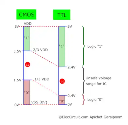
Voltages between and are in an undefined or "unsafe" region, where the gate's behavior is not guaranteed.
The image below illustrates these ranges for standard 5V TTL and CMOS.
The noise margins are calculated as the difference between the guaranteed output of a driving gate and the required input of a receiving gate:
- High Noise Margin () =
- Low Noise Margin () =
A larger noise margin is better.
As you can see in the diagram, CMOS has significantly wider noise margins than TTL. This is because its output can swing "rail-to-rail"—the logic '0' output is very close to 0V and the logic '1' is very close to the supply voltage. TTL outputs, due to the BJT structure, cannot pull the voltage as close to the supply rails.
The following videos will make these abstract numbers much more concrete.
What is TTL & CMOS? | TTL vs CMOS explained | TTL CMOS compatibility
The Blueprint IoT video provides a clear, animated explanation of these voltage bands and what they mean for noise margin.
Please watch the segment from this point. It breaks down the input and output thresholds for both TTL and CMOS and graphically shows why CMOS has a superior noise margin.
Next, let's watch a fantastic hands-on demonstration that shows these different voltage thresholds in a real circuit.
Exploring TTL and CMOS integrated circuits and some of their characteristics - #153
In this video, Lockdown Electronics uses a variable voltage source to find the exact input voltage at which a TTL gate and a CMOS gate flip their state, providing a powerful real-world example of the concepts we've just discussed.
Watch the following four clips: The TTL test, where he finds the logic-low threshold for a 74LS00 TTL chip. The CMOS test, where he does the same for a 4011 CMOS chip and compares the results. A brief explanation of the HC (High-Speed CMOS) family and its structural advantages. The final summary, which visualizes the results on a graph and discusses the different supply voltage requirements.
The different voltage levels have a critical practical implication: interfacing TTL and CMOS devices can be problematic. As the Blueprint IoT video will explain, a CMOS output can safely drive a TTL input, but a TTL output's guaranteed high voltage () may not be high enough to meet a standard CMOS gate's required high input voltage (). This can lead to unreliable operation.
Conclusion
In this lesson, we compared the two most influential logic families, TTL and CMOS, across three key performance axes. You now understand the engineering trade-offs that have made CMOS the technology of choice for modern digital electronics.
Here are the key takeaways:
- Underlying Technology: TTL uses current-controlled BJTs, while CMOS uses voltage-controlled MOSFETs.
- Power Consumption: TTL has significant static power draw. CMOS has negligible static power, but its dynamic power increases with frequency (). This makes CMOS ideal for battery-powered devices and high-density chips.
- Speed: While early TTL was faster, modern Advanced CMOS families (AC, AHC, LVC) match or exceed the speed of the fastest TTL families.
- Noise Margin: CMOS has superior noise immunity because its outputs swing rail-to-rail, creating larger voltage margins for both high and low logic levels compared to TTL.
You've now completed your journey through transistor-level logic, from single transistors to complete logic families. In the next module, "Combinational Logic Circuit Design," we will move up a level of abstraction. We'll start treating these gates as fundamental building blocks to design more complex and useful circuits like adders, multiplexers, and decoders, connecting more dots on your path to understanding embedded systems.
Can't find a good explanation? Sign up and we'll make it for you
Sign up