
Welcome back! In our last lesson, we delved into the Bipolar Junction Transistor (BJT), discovering how a small current at its base could control a much larger current flow, making it an effective electronic switch. You learned to analyze its behavior in the cut-off and saturation regions, establishing a solid foundation in transistor switching.
This lesson introduces the other titan of the transistor world: the Metal-Oxide-Semiconductor Field-Effect Transistor (MOSFET). While the BJT is current-controlled, the MOSFET is a voltage-controlled switch. This fundamental difference is the primary reason MOSFETs dominate modern digital electronics, from the powerful CPU in your computer to the humble microcontroller in a smart thermostat. Understanding this component is a pivotal step in your goal to see "how every dot connects," as it forms the building block for the integrated circuits we will study next.
From Current Control to Voltage Control
The most significant distinction between the BJT you just learned about and the MOSFET is how they are turned on and off.
- A BJT requires a continuous, albeit small, current flowing into its base to remain in the "ON" state. This constant current draw, while small, consumes power.
- A MOSFET, on the other hand, requires only a voltage to be applied to its gate terminal to turn "ON". The gate is insulated from the rest of the transistor, so in a steady "ON" or "OFF" state, it draws virtually no current.
This property of being voltage-controlled makes MOSFETs incredibly power-efficient, allowing billions of them to be packed into a single chip without generating unmanageable amounts of heat.
The following video uses a similar water-pipe analogy to the one we saw for BJTs, but it highlights this key difference in control.
MOSFET Explained - How MOSFET Works
The video "MOSFET Explained" by The Engineering Mindset provides an excellent high-level introduction to the MOSFET, contrasting it with the BJT and demonstrating its operation.
First, watch the introductory segment from the beginning, which includes a helpful water flow analogy for a voltage-controlled valve. Next, watch the section from here, which directly compares the current requirement of a BJT to the voltage requirement of a MOSFET, explaining why MOSFETs are more efficient.
The "Field-Effect": How It Works
The name "MOSFET" is a direct description of its structure: Metal-Oxide-Semiconductor. This structure is what enables the "Field-Effect" that gives the transistor its name. Let's focus on the most common type used in digital logic: the N-channel enhancement-mode MOSFET.
Its structure consists of:
- A P-type silicon substrate (the base material).
- Two heavily doped N-type regions, which form the Source and Drain terminals.
- A very thin insulating layer of Silicon Dioxide () grown over the substrate between the source and drain.
- A layer of conductive material (historically metal, now often polysilicon) on top of the oxide, which forms the Gate terminal.
Initially, with no voltage on the gate, there is no conductive path between the source and drain. The two N-regions are separated by the P-substrate, forming two back-to-back PN junctions that prevent current flow.
The magic happens when we apply a positive voltage to the gate relative to the source ().
The video "How Does a MOSFET Work?" from Explorer has exceptionally clear animations that show exactly what happens inside the semiconductor material.
Please watch the segment from this point. It visually walks you through the transition from the "OFF" state to the "ON" state. As you watch, pay close attention to these key steps: Cutoff: With zero gate voltage (V_{GS} = 0), notice how the depletion regions block any path for current. Channel Formation: When a positive V_{GS} is applied, see how the electric field attracts minority carriers (electrons) in the P-substrate. Inversion: As enough electrons accumulate under the gate, they form a thin N-type "channel" that connects the N-type source and drain. Now, current can flow.
This formation of a conductive channel using an electric field—without any current flowing into the control terminal—is the core principle of the MOSFET. The minimum gate-source voltage needed to form this channel is called the threshold voltage ().
The MOSFET as a Digital Switch
Just as with the BJT, for digital applications, we operate the MOSFET in its two extreme states: fully OFF or fully ON. These correspond to the Cut-off and Saturation regions. The article below provides a clear definition of these states, creating a direct parallel to the BJT lesson.
Use a MOSFET as a Switch - Electronics Tutorials
This article from Electronics-Tutorials.ws defines the operating regions for an enhancement-mode MOSFET when used as a switch.
Start by reading the introduction and the section on The Enhancement-mode MOSFET to get an overview. Next, read section 1, The Cut-off Region. Note the condition: V_{GS} < V_{th}. In this state, the MOSFET acts as an open switch. Finally, read section 2, The Saturation Region. Note the condition: V_{GS} > V_{th}. In this state, the MOSFET's channel has very low resistance (R_{DS(on)}) and acts as a closed switch.
To summarize for switching purposes:
-
Cut-off Region (OFF):
- Condition: Gate-Source Voltage is less than the threshold voltage ().
- Behavior: No conductive channel exists. The resistance between drain and source is extremely high.
- Analogy: An open switch.
-
Saturation Region (ON):
- Condition: Gate-Source Voltage is significantly greater than the threshold voltage ().
- Behavior: A strong conductive channel is formed. The resistance between drain and source, known as , is very low.
- Analogy: A closed switch.
N-Channel and P-Channel MOSFETs
So far, we've discussed the N-channel MOSFET. Its counterpart is the P-channel MOSFET, which operates in a complementary fashion. The ability to use both types together is the foundation of modern, low-power CMOS (Complementary MOS) logic, which we will explore in the next lesson.
Here’s a comparison:
| Feature | N-Channel MOSFET | P-Channel MOSFET |
|---|---|---|
| Structure | N-type source/drain in a P-type substrate. | P-type source/drain in an N-type substrate. |
| Charge Carriers | Electrons | Holes |
| Turn-ON Voltage | Positive () | Negative () |
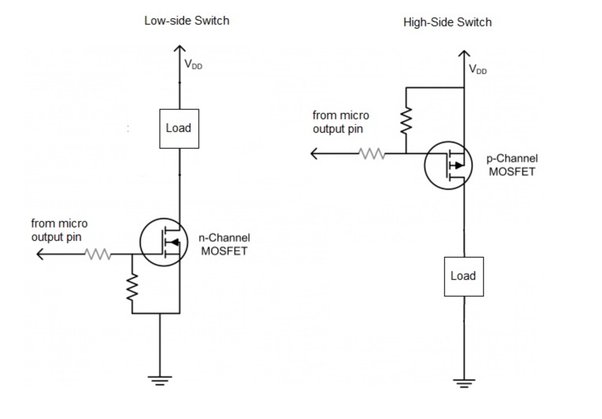
| Common Use | Low-side switch (connects load to Ground) | High-side switch (connects load to ) |
The image below illustrates the difference in structure, current flow, and circuit symbols for both types.
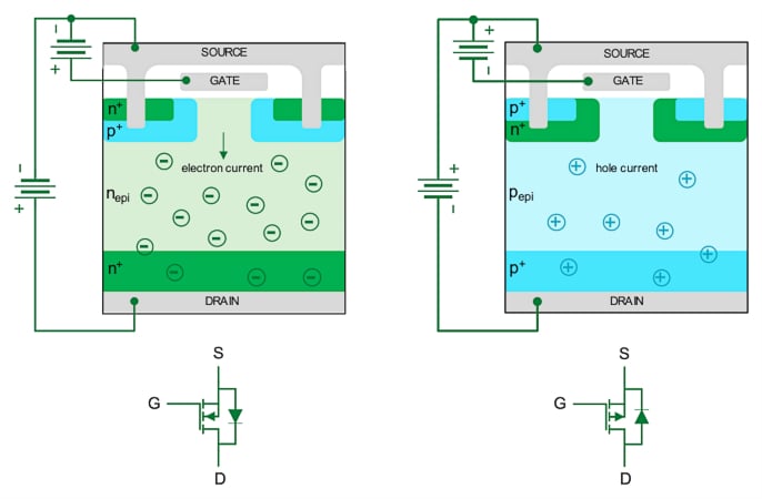
This difference in control polarity leads to their typical use in circuits. Because the control voltage () is referenced to the source, it's often easiest to drive an N-channel MOSFET when its source is connected to ground. This creates a low-side switch. Conversely, a P-channel MOSFET is most easily used as a high-side switch, with its source connected to the positive voltage supply.
Conclusion
In this lesson, you have been introduced to the MOSFET, the workhorse of modern digital electronics. You've moved beyond the current-controlled BJT to understand the principles of a voltage-controlled switch, a critical concept for building the low-power, high-density circuits that define modern computing.
Key takeaways from this lesson are:
- A MOSFET is a voltage-controlled switch, where a voltage applied to the gate controls the flow of current between the drain and source.
- Its operation relies on the field-effect: an electric field from the gate voltage creates a conductive channel in the semiconductor material.
- The insulating oxide layer at the gate means there is virtually no steady-state gate current, making MOSFETs extremely power-efficient compared to BJTs.
- For switching, a MOSFET is operated in two main regions:
- Cut-off (OFF): When , it acts as an open switch.
- Saturation (ON): When , it acts as a closed switch with a low on-resistance ().
- N-channel and P-channel MOSFETs are complementary devices, turned on by positive and negative gate-source voltages, respectively. This makes them ideal for low-side and high-side switching applications.
You now understand how both BJT and MOSFET transistors can act as switches. In the next lesson, we will take the crucial next step up the ladder of abstraction. You will see how N-channel and P-channel MOSFETs are combined to create the fundamental logic gates—NAND and NOR—that form the basis of all digital computation.
Can't find a good explanation? Sign up and we'll make it for you
Sign up