Hello Alex,
Welcome back to our course. In the previous lesson, we analyzed the MOSFET's I-V characteristics, defining the cutoff, triode, and saturation regions with their corresponding equations. We saw how the gate voltage controls the flow of current , and how the device can behave as an open circuit, a resistor, or a current source.
Today, we'll focus on the first major application of this behavior: using the MOSFET as a digital switch. You'll see how the sharp distinction between the "OFF" (cutoff) and "ON" (triode) states makes the MOSFET the perfect element for constructing the logic gates that are the foundation of all modern digital electronics. As a developer, you work with logical constructs like if, AND, OR, and NOT every day; this lesson reveals the physical hardware that brings that logic to life.
Learning Outcome: The MOSFET as a Switch in Digital Logic
Approximate time to complete: 50 minutes.
1. The MOSFET as a Voltage-Controlled Switch
Let's quickly recap the two states that are crucial for digital logic:
- Cutoff (OFF) State: When , no channel forms. The MOSFET acts as an open switch, and ideally, no current flows between the drain and source. We can associate this with a logical 0 input causing an OFF state.
- Triode/Ohmic (ON) State: When and is small, a conductive channel forms. The MOSFET acts as a closed switch with a low resistance (). A logical 1 input causes an ON state, creating a path for current.
The goal in digital logic is to use these ON/OFF states to produce a high voltage (logical '1') or a low voltage (logical '0') at an output terminal.
2. The CMOS Principle: Complementary Switches
While you can build a rudimentary switch with just one NMOS transistor and a resistor, this approach is inefficient and suffers from power loss. Modern digital circuits overwhelmingly use CMOS (Complementary Metal-Oxide-Semiconductor) logic. The "complementary" part is the key. It involves using a pair of transistors—one N-channel MOSFET (NMOS) and one P-channel MOSFET (PMOS)—that work in opposition.
Let's watch a short video that introduces how these two transistor types behave as electrically controlled switches.

- Watch: N-MOS and P-MOS Transistor as Electrically Controlled Switches (00:00 - 03:01).
As the video explains, their behavior is perfectly complementary:
- NMOS Transistor:
- Gate = HIGH (1): The switch is ON (closed). It creates a low-resistance path to Ground.
- Gate = LOW (0): The switch is OFF (open).
- PMOS Transistor:
- Gate = LOW (0): The switch is ON (closed). It creates a low-resistance path to the high supply voltage, VDD.
- Gate = HIGH (1): The switch is OFF (open).
Notice that for any given input, one type is ON while the other is OFF. This is the genius of CMOS.
3. The CMOS Inverter (The NOT Gate)
The most fundamental logic gate is the inverter, or NOT gate. It's built by connecting one PMOS and one NMOS transistor as shown below. The PMOS forms the "pull-up network" (connecting the output to VDD), and the NMOS forms the "pull-down network" (connecting the output to Ground).
CMOS Inverter Circuit
A CMOS Inverter connects a PMOS and an NMOS transistor. The input is tied to both gates, and the output is taken from the connected drains.

Let's analyze its operation and, crucially, understand why it's so power-efficient.
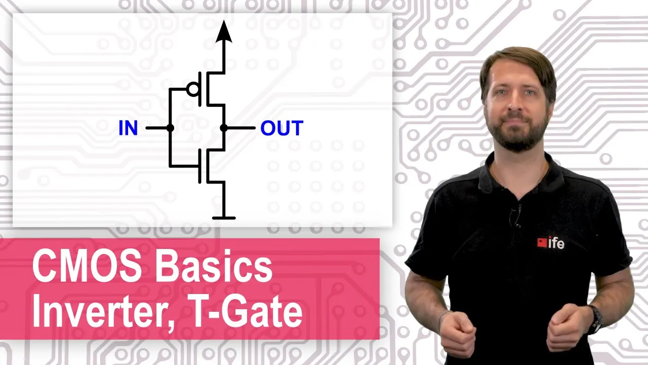
- Watch: CMOS Inverter as a Digital Switch (01:52 - 05:00).
The video beautifully contrasts the CMOS approach with the older, inefficient resistor-transistor logic (RTL). Now let's trace the logic of our CMOS inverter:
-
Case 1: Input is HIGH (Logical 1)
- The NMOS gate receives a HIGH voltage, so it turns ON, creating a direct path from the output to Ground.
- The PMOS gate also receives a HIGH voltage, so it turns OFF, breaking the path to VDD.
- Result: The output is pulled LOW (Logical 0).
-
Case 2: Input is LOW (Logical 0)
- The NMOS gate receives a LOW voltage, so it turns OFF.
- The PMOS gate receives a LOW voltage, so it turns ON, creating a direct path from the output to VDD.
- Result: The output is pulled HIGH (Logical 1).
The Power Advantage: In either stable state (input held HIGH or LOW), one of the transistors is always OFF. This means there is no direct path for current to flow from VDD to Ground. This is why CMOS circuits have near-zero static power consumption, a revolutionary feature that enabled the development of dense, low-power microchips in everything from your phone to your laptop. Power is primarily consumed only during the brief moment of switching.
4. Building NAND and NOR Gates
Now that we understand the inverter, we can build more complex gates like NAND and NOR, which are the universal building blocks for all other digital logic. The key is a design principle of duality:
- If the pull-up network (PMOS) uses transistors in series, the pull-down network (NMOS) must use them in parallel.
- If the pull-up network uses transistors in parallel, the pull-down network must use them in series.
The EngMicroLectures video provides a clear, step-by-step construction of both.
A. The CMOS NAND Gate
Let's see how to build a 2-input NAND gate. Remember, a NAND gate's output is LOW only when both inputs A and B are HIGH.
- Watch: from 04:10 to 08:06.
As the video demonstrates, the structure is:
- Pull-up (PMOS): Two PMOS transistors connected in parallel. If either A or B is LOW, at least one PMOS is ON, pulling the output HIGH.
- Pull-down (NMOS): Two NMOS transistors connected in series. The path to ground is complete only if both A and B are HIGH, turning both NMOS transistors ON.
This perfectly implements the NAND logic while preserving the low-power CMOS principle.
B. The CMOS NOR Gate
Next, the NOR gate. Its output is HIGH only when both inputs A and B are LOW.
- Watch: from 08:06 to 10:49.
As you'll see, the NOR gate's structure is the dual of the NAND gate:
- Pull-up (PMOS): Two PMOS transistors in series. The path to VDD is complete only if both A and B are LOW, turning both PMOS transistors ON.
- Pull-down (NMOS): Two NMOS transistors in parallel. If either A or B is HIGH, at least one NMOS is ON, pulling the output LOW.
From these simple patterns, any digital logic function can be constructed.
5. Advanced Topic: The Transmission Gate
Besides building logic gates, the complementary nature of CMOS allows for another powerful component: the transmission gate. This acts as a bidirectional electronic switch, controlled by a logic signal. It's used extensively in circuits like analog multiplexers and sample-and-hold circuits.
- Watch: from 05:55 to 08:28.
This circuit uses an NMOS and a PMOS in parallel to pass a signal. When the control signal is HIGH, both transistors turn on, allowing the signal to pass through in either direction. When the control signal is LOW, both turn off, blocking the signal. This is another elegant application of the MOSFET as a switch.
Conclusion
In this lesson, you've seen how the simple ON/OFF behavior of MOSFETs, when combined in complementary pairs, forms the basis of all modern digital logic.
Key Takeaways:
- MOSFETs are ideal digital switches, using the cutoff region for OFF and the triode region for ON.
- CMOS logic uses complementary pairs of NMOS and PMOS transistors. This design is extremely power-efficient because there is no static current path from the power supply (VDD) to Ground.
- The inverter (NOT gate) is the fundamental CMOS building block.
- More complex gates like NAND and NOR are created using series and parallel combinations of transistors, following a principle of duality between the NMOS pull-down network and the PMOS pull-up network.
We have now seen how to use the cutoff and triode regions for digital circuits. In our next lesson, we will shift our focus to analog electronics and explore "The MOSFET Common-Source Amplifier". There, you will see how the saturation region, where the MOSFET acts as a voltage-controlled current source, is used to amplify signals.