Hello Alex,
Welcome back. In our previous lesson, we explored how MOSFETs are used as digital switches by leveraging their behavior in the cutoff (OFF) and triode (ON) regions. This is the foundation of the digital logic that powers the software you write every day.
Today, we shift our focus from digital to analog electronics. We will investigate how the MOSFET, when operated in its saturation region, functions as an amplifier. You'll learn about the most fundamental MOSFET amplifier topology: the common-source amplifier. This configuration is the cornerstone of many analog circuits used in radio receivers, sensors, and communication systems.
This lesson will connect directly with your background in Radiophysics, as we'll perform the classic DC and AC analyses that are essential for characterizing any amplifier stage.
Learning Outcome: The MOSFET Common-Source Amplifier: Biasing and Small-Signal Analysis
Approximate time to complete: 60 minutes.
1. The Amplifier's Goal: From Switch to Signal Booster
For an amplifier, we don't want the abrupt ON/OFF behavior of a switch. Instead, we want the output to be a magnified, linear reproduction of the input. To achieve this, we must operate the MOSFET in the saturation region.
Recall that in saturation, the drain current is controlled by the gate-source voltage but is almost independent of the drain-source voltage . The MOSFET acts as a voltage-controlled current source. A small change in the input voltage () produces a proportional change in the drain current (). By passing this changing current through a resistor, we can convert it into a much larger change in output voltage.
2. DC Analysis: Setting the Stage with Biasing
Before we can amplify an AC signal, we must set up the correct DC operating conditions. This process is called biasing. The goal is to establish a stable DC operating point, or Quiescent Point (Q-point), that places the transistor squarely in the middle of its saturation region. This ensures the AC signal can swing both up and down without being clipped or distorted by accidentally entering the triode or cutoff regions.
Let's start with a simple common-source amplifier circuit with a resistive load and analyze its DC behavior.
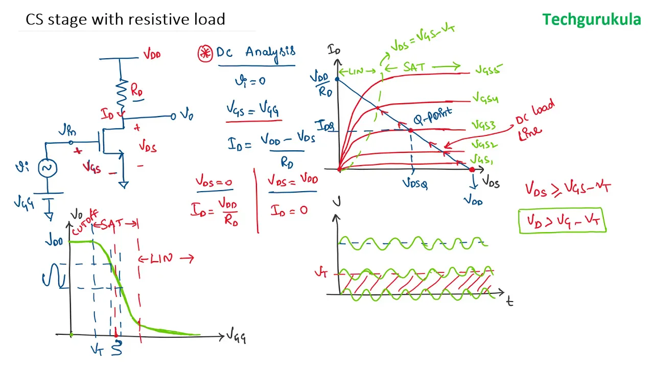
- Watch: MOSFET Common Source Amplifier Circuit and DC Biasing (00:00 - 04:27).
As the video explains, we can analyze the DC conditions using a load-line analysis, a classic technique you may remember from your studies.
-
The load line represents all possible operating points for the output loop. It's derived from Kirchhoff's Voltage Law (KVL) around the drain circuit:
This is the equation of a straight line on the MOSFET's vs. characteristic curves. -
The Q-point () is the intersection of this load line with the specific curve corresponding to our chosen DC bias voltage, .
Our primary goal during biasing is to select and such that this Q-point satisfies the saturation condition:
The video continues to show the transfer characteristic ( vs. ), which graphically illustrates why the saturation region provides amplification.
- Watch: Transfer Characteristics and Biasing Considerations (04:27 - 09:40).
Notice the steep, almost linear slope in the saturation region. A small change in the input voltage here causes a large change in the output voltage, which is exactly what we want from an amplifier. The negative slope also tells us that the output signal will be an inverted version of the input—a 180° phase shift.
3. AC Analysis: The Small-Signal Model
With the DC Q-point established, we can now analyze how the circuit responds to a small AC input signal, , that "rides on top" of the DC bias. We use the small-signal model, which linearizes the MOSFET's behavior around the Q-point.
The two key parameters of this model are:
- Transconductance (): This relates the change in output current to the change in input voltage. It's the "gain" of the transistor itself.
- Output Resistance (): This models the slight dependence of on in saturation (channel-length modulation). For many analyses, it's large enough to be ignored, but for precision, we include it. .
To perform AC analysis, we create an AC equivalent circuit:
- All DC voltage sources are treated as AC ground.
- All large capacitors (for coupling and bypass) are treated as short circuits.
- The MOSFET is replaced by its small-signal model.
Let's see this process in action to find the amplifier's gain.
- Watch: Small-Signal AC Analysis: Equivalent Circuit and Gain Derivation (09:40 - 12:50) from the
techgurukulavideo.
The derivation leads to the crucial formula for voltage gain ():
The term represents the total effective AC resistance seen at the drain terminal. The negative sign confirms the 180° phase inversion we predicted earlier.
4. Input and Output Resistance
Besides gain, two other critical parameters define an amplifier's behavior.
- Input Resistance (): How much the amplifier "loads" the signal source.
- Output Resistance (): The internal resistance of the amplifier as seen from the output.
The video zQZ3D also covers how to find these.
- Watch: Input and Output Resistance Analysis (12:50 - 14:59).
Input Resistance ()
For the simple circuit shown, we are looking into the gate of the MOSFET. Since the gate is insulated by a layer of oxide, it presents an open circuit to the input signal.
This extremely high input resistance is a major advantage of MOSFET amplifiers, as they draw virtually no current from the signal source.
Output Resistance ()
Looking back into the output terminal (with the input source turned off), we see the MOSFET's own output resistance in parallel with the drain resistor .
5. A More Practical Biasing Circuit: Voltage Divider Bias
The simple biasing scheme we first analyzed is sensitive to variations in transistor parameters. A more robust and common method is voltage divider biasing, which you may have also seen in BJT circuits.

This circuit uses resistors and to create a stable DC voltage at the gate, and a source resistor to provide negative feedback for DC stability. For AC analysis, a large bypass capacitor is often placed in parallel with to "short it out" for the AC signal, preventing it from reducing the gain.
- Watch: DC Analysis for GM Calculation (01:07 - 05:42).
This video walks through the DC analysis needed to find the Q-point and thus the transconductance for this more practical circuit. The key equations to solve simultaneously are:
- Gate Voltage:
- Gate-Source Loop:
- Transistor Equation:
Solving this system gives you the DC operating point (), from which you can calculate .
The AC analysis for this circuit (with bypassing ) is very similar to what we've already done. The source is at AC ground, and the gain is approximately , where is the load resistance. The key difference is the input resistance is now dominated by the biasing resistors: .
Conclusion
In this lesson, you have analyzed the common-source amplifier, the workhorse of analog MOSFET circuits. We have moved from the digital world of ON/OFF states to the analog world of signal amplification by harnessing the MOSFET's behavior in the saturation region.
Key Takeaways:
- The common-source amplifier provides voltage gain by operating the MOSFET in the saturation region, where it acts as a voltage-controlled current source.
- DC biasing is essential to establish a stable Q-point () that allows for maximum undistorted signal swing.
- AC small-signal analysis allows us to model the amplifier's behavior for AC signals and derive its key characteristics.
- The voltage gain is approximately , where is the total AC resistance at the drain. The negative sign signifies a 180° phase inversion.
- The CS amplifier has a very high input resistance, making it easy to drive, and a moderate output resistance.
This lesson concludes our module on the fundamentals of transistors. You've seen how both BJTs and MOSFETs can function as switches and amplifiers. We will now move to a higher level of abstraction in analog circuit design. In the next lesson, we will begin our study of the Operational Amplifier (Op-Amp), an incredibly versatile building block that uses many internal transistors but can be analyzed with a few simple, powerful rules.