
Good to see you again. In the previous lesson, roofline analysis treated a kernel as FLOPs plus bytes moved, then asked whether compute throughput or high-bandwidth memory bandwidth sets the ceiling. This lesson explains the machinery behind those bytes and FLOPs: how CUDA maps a large grid of logical threads onto GPU hardware, how an SM runs them as warps, and where their data lives while they execute.
By the end, you should be able to trace a thread block from kernel launch through warp scheduling and identify the path from device memory into caches, shared memory, registers, execution units, and back. This is the hardware model needed to reason credibly about occupancy, divergence, reuse, and the memory-access optimizations that follow.
From a grid to a resident thread block
A CUDA kernel launch creates a grid: potentially millions of logical threads arranged into thread blocks. Blocks may be one-, two-, or three-dimensional, but their most important role is structural:
- Threads within one block can cooperate through shared memory and block-level synchronization.
- A block is assigned to one Streaming Multiprocessor, or SM, for its execution.
- Different blocks are independent. CUDA does not guarantee their scheduling order, or even that two particular blocks run concurrently.
That final property is what lets one kernel run correctly on a small GPU with relatively few SMs and on a large GPU with many more. A larger GPU simply makes more blocks resident at once.
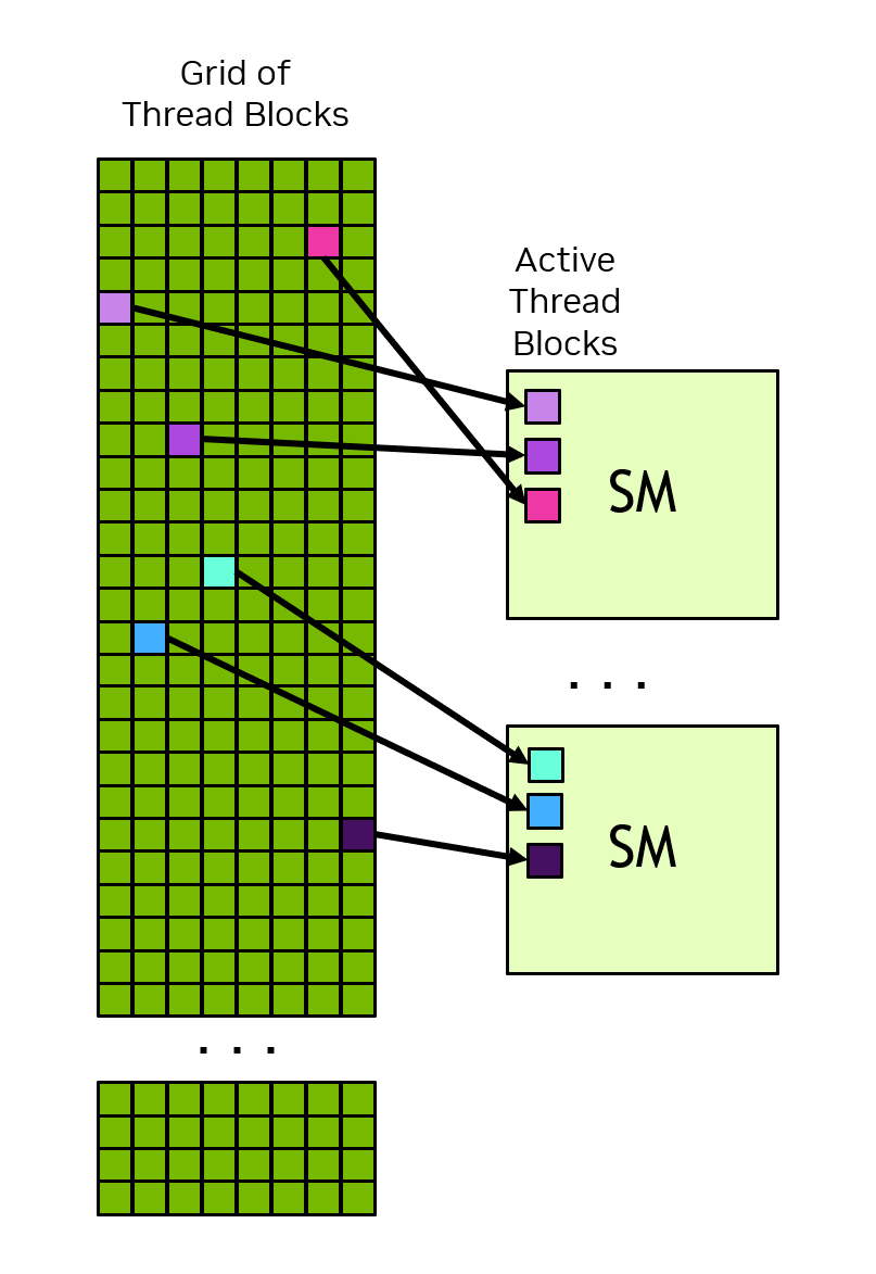
Suppose a vector-add kernel launches 1,024 blocks with 256 threads each. The kernel contains 262,144 logical threads, but a GPU does not need that many physical arithmetic lanes. Instead:
- The runtime makes blocks eligible to execute.
- Each SM receives as many blocks as its resources permit.
- Those blocks remain on the SM until completion.
- The SM divides their threads into warps and schedules those warps over time.
- When a block completes, another block can take its place.
A block’s resource needs determine how many blocks can coexist on an SM. The important resources are:
- threads and warps;
- registers;
- shared memory;
- hardware limits on resident blocks and resident warps.
This coexistence is called residency. It is not the same as all resident threads executing simultaneously. An SM keeps many warps ready, then issues instructions from whichever warp can make progress.
Understanding NVIDIA GPU Hardware as a CUDA C Programmer | Episode 2: GPU Compute Architecture
Watch “Understanding NVIDIA GPU Hardware as a CUDA C Programmer,” by Tushar Gautam, for a visual first pass through block placement, warp formation, latency hiding, and shared memory.
Watch block to warp mapping. Focus on the distinction between logical grid layout and arbitrary block scheduling onto SMs, then on why a block is subdivided into 32-thread warps. Then skip ahead and watch latency and shared memory, focusing on why an SM needs many available warps and why explicitly staged on-chip data can reduce device-memory traffic.
For a precise CUDA-level account, use the Programming Guide sections below. They establish the execution and memory scopes that you should use in an interview or system-design discussion, rather than treating the diagram as a literal physical floor plan.
1.2. Programming Model — CUDA Programming Guide
Read NVIDIA's CUDA Programming Guide to establish the durable programming-model guarantees: a block executes on one SM, blocks are independently scheduled, and memory spaces have distinct scopes.
In Section 1.2.2.1, “Thread Blocks and Grids,” read block scheduling. Pay particular attention to why inter-block dependencies are invalid within an ordinary kernel launch. Then move to Section 1.2.3.2, “On-Chip Memory in GPUs.” Read on-chip memory, and continue into subsection 1.2.3.2.1, “Caches,” reading the cache hierarchy. Distinguish an address space such as global memory from the cache levels that may accelerate access to it.
The warp: the SM's unit of scheduling
A block is the programmer-facing cooperation unit; a warp is the core execution unit.
CUDA partitions every block into groups of 32 consecutive threads:
where is the number of threads in the block.
For example, a 256-thread block becomes eight warps. In a one-dimensional block, warp 0 contains threads 0 through 31, warp 1 contains threads 32 through 63, and so on. For a two-dimensional block, CUDA conceptually linearizes thread IDs with the dimension varying fastest, then partitions that sequence into warps.
Each thread has its own:
- thread index and computed data index;
- registers and intermediate values;
- memory addresses;
- control-flow state.
But a warp executes in the SIMT model: Single Instruction, Multiple Threads. At a given issue opportunity, the SM selects a ready warp and dispatches one instruction for its active lanes. Conceptually, this resembles 32 threads performing the same instruction over 32 independent values.
Consider:
if (x[i] > 0) {
    y[i] = x[i];
} else {
    y[i] = 0;
}
If every lane in a warp takes the same branch, the warp executes efficiently. If 16 lanes take the first path and 16 take the second, the warp must execute both paths, masking off the lanes not participating in each path. This is warp divergence.
Divergence is therefore a within-warp issue:
- Different warps may execute completely different code paths without directly causing each other to serialize.
- Within one warp, different paths consume separate execution opportunities.
- A conditional at the boundary of a tensor is often harmless if only the final warp is affected.
- A data-dependent branch throughout a large tensor can be costly when adjacent threads commonly take different paths.
A thread-block size that is not a multiple of 32 is legal, but the last warp has permanently inactive lanes. A 250-thread block still consumes eight warps, but its eighth warp has only 26 useful threads. Choosing block sizes such as 128, 256, or 512 often avoids this particular waste, although it does not by itself guarantee good performance.
Modern NVIDIA GPUs support independent thread scheduling, so software must not rely on an old informal assumption that every warp lane reaches every instruction at exactly the same moment. When threads cooperate at warp scope, CUDA provides explicit primitives such as __syncwarp(). For block-wide shared-memory cooperation, use __syncthreads().
A thread's memory hierarchy
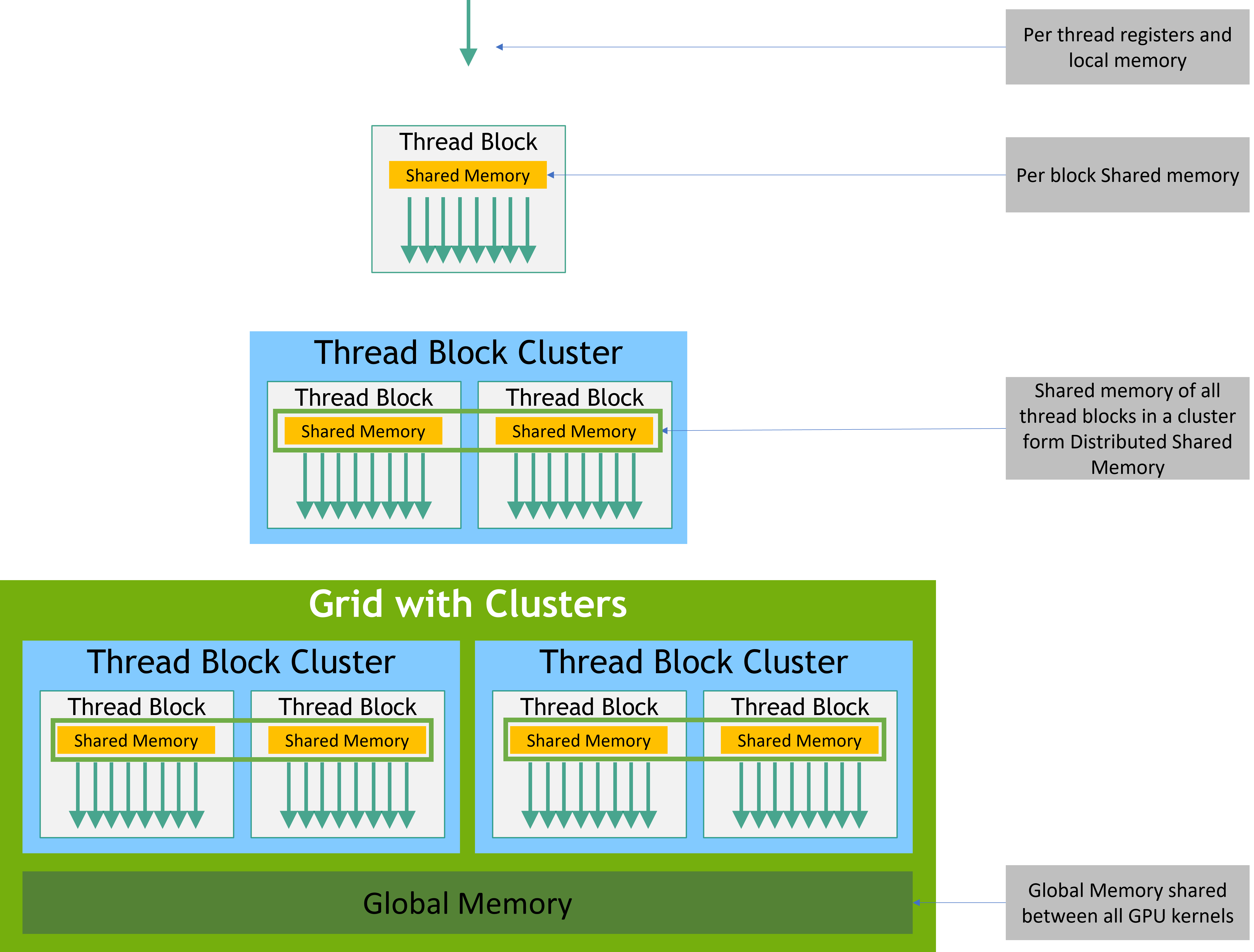
The word “memory” hides several distinct resources. Their differences in scope, capacity, latency, and programmability determine whether a kernel obtains reuse or repeatedly pays for device-memory traffic.
Registers: private working state
Registers are on-chip storage assigned to individual threads, usually by the compiler. A thread’s loop counter, address calculations, partial sum, and temporary operands often live there.
A typical arithmetic instruction follows this path:
For example, in a matrix multiplication kernel, each thread may retain one or more output partial sums in registers while iterating over a tile. Keeping those accumulators in registers avoids repeatedly storing and reloading them from shared memory or HBM.
Registers are extremely fast, but not unlimited. If a kernel uses registers per thread and has threads per block, a simplified register allocation estimate is:
For a kernel using 96 32-bit registers per thread and 256 threads per block:
If an SM had 65,536 registers available, register capacity alone would permit at most:
such blocks. Actual residency can be lower because shared memory, warp limits, and allocation granularity also apply.
When the compiler cannot keep all needed private values in registers, it may spill some values to local memory. The name is potentially misleading: local memory has per-thread scope, but is generally backed by device memory and accessed through the cache hierarchy. Register spills can therefore introduce much slower loads and stores. High register use is not automatically bad, because it can avoid spills and enable useful computation, but it is a major occupancy trade-off.
Shared memory: explicit block-level reuse
Shared memory is programmable on-chip storage allocated per block. Every thread in that block can read and write it.
Its common purpose is to stage data that multiple threads will reuse:
Threads often follow this sequence:
- Cooperatively load a tile from global memory into shared memory.
- Synchronize, ensuring the tile is fully available.
- Reuse values from shared memory across many arithmetic operations.
- Synchronize again before overwriting the shared-memory storage with the next tile.
Shared memory enables both communication and reuse, but it consumes a limited resource at block granularity. A kernel that allocates too much shared memory per block may reduce the number of resident blocks and warps. It also requires correct synchronization: a thread must not read another thread’s shared-memory write before the producer has completed it.
On modern GPUs, shared memory and the per-SM L1 cache draw from related on-chip hardware resources. The exact capacity split and implementation vary by GPU architecture. At the programming-model level, the key distinction remains clear:
- shared memory is explicitly managed by the kernel;
- L1 is a hardware-managed cache.
Caches: automatic reuse
Caches can serve global-memory accesses without changing the memory scope or correctness model.
- L1 cache is associated with an SM and can satisfy some accesses made by warps executing there.
- L2 cache is shared across the GPU's SMs.
- A global-memory access that misses in relevant caches proceeds to device DRAM.
Caches are valuable when the hardware detects temporal or spatial locality, but a kernel should not require a particular cache hit for correctness. In performance analysis, cache effects also explain why actual HBM traffic can be less than a simplistic “bytes referenced by source code” calculation.
Global memory: GPU device DRAM, often HBM
CUDA calls the DRAM attached to a GPU global memory because all SMs on that GPU can address it. In many data-center accelerators, this DRAM is HBM, high-bandwidth memory.
Global memory is large and offers enormous aggregate bandwidth, but its access latency is much higher than on-chip storage. HBM is “high bandwidth,” not “low latency.” A single warp that issues a load to HBM may wait hundreds of cycles before its operands are ready.
A global-memory load is best understood as a request with several possible outcomes:
The exact microarchitecture differs by GPU generation, but this is the right conceptual path. In the reverse direction, stores originate from registers, travel through the memory system, and eventually update global memory.
One warp executing a simple kernel
Consider a simplified vector-add kernel:
i = blockIdx.x * blockDim.x + threadIdx.x;

if (i < n) {
    c[i] = a[i] + b[i];
}
Trace warp 0 of a 256-thread block:
-
Thread identity enters registers.
Each lane obtains its own thread and block identifiers, then computes its own global index . The instructions are common across the warp, but the register values differ per lane. -
The warp forms global-memory addresses.
Lane 0 requestsa[i]andb[i]for its index; lane 1 requests the next elements; and so on. When neighboring threads access neighboring addresses, hardware can combine the requests into relatively few memory transactions. This is coalescing, the next lesson's central topic. -
The load instruction may stall this warp.
The requested values might arrive from L1, L2, or HBM. Until the required values arrive in registers, this warp is not ready to execute the addition. -
The warp scheduler issues another ready warp instead.
The SM has retained register state and execution context for many resident warps. Switching among them does not require a CPU-style context switch. While warp 0 waits for memory, warp 3 might execute arithmetic, warp 6 might issue another load, and so on. -
Operands arrive in registers.
Warp 0 becomes ready. The SM can issue the addition, producing each lane's result in its registers. -
The warp stores results to global memory.
Each active lane writesc[i]. The store request moves through the memory hierarchy, while the warp may proceed if it has independent work.
This is the central GPU latency-hiding mechanism: do not wait idly for one warp's long-latency load when another warp can execute.
That leads to an important distinction:
- Bandwidth concerns how many bytes per second the GPU can sustain.
- Latency concerns how long one access takes to return.
- Occupancy concerns the fraction of hardware-supported warps that are resident.
- Useful latency hiding depends on having enough ready warps with independent work, not merely a high occupancy percentage.
A kernel can have high nominal occupancy and still be slow because its accesses are inefficient or its arithmetic intensity is low. Conversely, a kernel can have moderate occupancy but perform well if it has enough ready work and benefits from substantial register reuse.
A tiled matrix multiplication: all memory levels working together
The vector-add trace uses little data reuse, so it is usually memory-bandwidth-bound. A tiled matrix multiplication shows why registers and shared memory matter for AI workloads.
Suppose a block computes a tile of output matrix :
Use 256 threads per block, with one thread conceptually responsible for one output element. The block contains eight warps. Rather than having every thread repeatedly fetch values directly from global memory, the block iterates over tiles along the reduction dimension.
For each tile iteration:
-
Cooperative global loads
Threads load a tile from and a corresponding tile from from global memory into shared memory. A good mapping arranges adjacent lanes to access adjacent addresses. -
Block-level synchronization
All threads wait at__syncthreads()before consuming the tile. This ensures no thread begins reading a shared-memory element before its producer has written it. -
Shared-memory reads and register accumulation
Each thread repeatedly reads values from the shared tiles. It multiplies them and adds the products into an accumulator held in a register. -
Second synchronization
Before the shared-memory arrays are reused for the next pair of tiles, threads synchronize again so that no thread overwrites data another thread still needs. -
Final global store
After all reduction tiles are processed, each thread writes its register-held result to the appropriate output location in global memory.
The benefit is multiplicative reuse. A value loaded once from global memory into shared memory can contribute to many output calculations. A partial output sum stays in a register across many multiply-adds. The result is less HBM traffic per FLOP, which raises arithmetic intensity:
That is the physical mechanism behind the roofline lesson's high-intensity matrix-multiplication case.
In practice, high-performance GEMM and attention kernels add much more sophistication: careful thread layouts, tensor-core instructions, asynchronous copies, deeper pipelining, and register tiling. But the basic dataflow remains:
A practical trace for performance reasoning
When diagnosing a CUDA kernel, walk through this sequence rather than jumping immediately to a favored optimization:
-
Map work to blocks.
What output region or token subset does each block own? Does the algorithm require illegal communication across independently scheduled blocks? -
Map block threads to warps.
Is the block size a multiple of 32? Do threads that share a warp usually follow the same control path? -
Identify each value's natural home.
- Private short-lived values and accumulators: registers.
- Values reused among block threads: shared memory.
- Large tensors and final outputs: global memory.
- Repeated, hardware-managed reuse: caches.
-
Estimate resource pressure.
How many registers per thread and bytes of shared memory per block are required? Do those allocations prevent enough warps from becoming resident to hide latency? -
Trace global loads and stores.
Are neighboring warp lanes accessing neighboring addresses? Are values fetched once and reused, or repeatedly fetched from HBM? -
Connect the trace to the roofline.
Excess global-memory traffic increases the byte term , decreases arithmetic intensity, and makes a kernel more likely to be memory-bound. Better reuse through registers, caches, or shared memory can reduce HBM traffic and move the kernel toward the compute roof.
For LLM systems, this explains a recurring pattern. Large training or prefill matrix multiplications can extract substantial reuse from weights and activations, while decode at small batch sizes frequently streams large weights for relatively little work. The latter tends to expose device-memory bandwidth and latency much more directly.
Key takeaways
- A CUDA grid contains blocks; a block is assigned to one SM; an SM may host multiple active blocks, subject to register, shared-memory, and warp limits.
- Each block is partitioned into 32-thread warps. Warps are the SM's scheduling units.
- In SIMT execution, active lanes in a warp execute a common instruction. Divergent branch paths are serialized within that warp through lane masking.
- Registers provide private, on-chip thread state and are ideal for temporary values and accumulators. Excess register demand can reduce residency or cause costly local-memory spills.
- Shared memory is explicit, on-chip storage shared by a block. It enables cooperation and reuse but requires synchronization and consumes a per-block resource budget.
- L1 and L2 caches automatically accelerate some global-memory accesses; global memory is GPU device DRAM, often HBM, with enormous bandwidth but substantial latency.
- When a warp waits on a memory operation, the SM can issue work from another ready warp. Sufficient useful warp-level concurrency hides latency.
- The next performance question is whether a warp's global-memory accesses combine efficiently into memory transactions. Next, you will determine whether a GPU access pattern is coalesced and use that analysis to identify avoidable HBM traffic.
Can't find a good explanation? Sign up and we'll make it for you
Sign up