
In our previous lesson, we established the fundamental concept of semiconductor doping, transforming pure silicon into N-type and P-type materials, each with a specific type of mobile charge carrier. This was the first crucial step in understanding how the physical properties of a material can be engineered for computation. Now, we will take the next logical step and see what happens when these two materials are brought together.
This lesson focuses on the PN junction, the interface where P-type and N-type silicon meet. You will learn how this simple junction forms a device with a remarkable property: it allows electric current to flow in only one direction. This device, the diode, is not just a theoretical curiosity; it's a foundational component in nearly all electronic circuits. We will explore how a diode behaves under different voltage conditions and examine its role in simple, yet essential, circuits, including a first look at how physical components can implement the logic gates you're already familiar with.
The Unbiased PN Junction: A State of Equilibrium
When a P-type and an N-type semiconductor are joined, an immediate and fascinating process begins at the interface, even with no external voltage applied. The N-type side has a high concentration of free electrons, and the P-type side has a high concentration of holes. This concentration difference drives a process called diffusion.
- Electrons from the N-side diffuse across the junction to the P-side, where they find and combine with holes.
- Holes from the P-side diffuse across to the N-side, where they combine with electrons.
This process is called recombination. As electrons leave the N-side and holes leave the P-side, they leave behind the fixed, immobile donor and acceptor ions we discussed in the last lesson. This creates a region near the junction that is depleted of mobile charge carriers. This area is fittingly called the depletion region or space-charge region.
The uncovered positive ions on the N-side and negative ions on the P-side create an electric field across the junction. This field results in a built-in potential barrier that opposes any further diffusion of majority carriers. Eventually, an equilibrium is reached.
The following video from Neso Academy provides an excellent, detailed explanation of this process. It breaks down the formation of the depletion region and the two opposing currents—diffusion current and drift current—that result in a net zero current in this unbiased state.
PN Junction Diode (No Applied Bias)
This video explains the physics of what happens at a PN junction when no external voltage is applied. Understanding this equilibrium state is key to understanding how a diode works when we do apply voltage.
Please watch from the beginning of the explanation to the end. Pay close attention to these key concepts: Diffusion Current: Why majority carriers (electrons and holes) initially cross the junction (see here). Depletion Region: How recombination leads to a region with only immobile ions (formation explained). Barrier Potential: How the electric field across the depletion region opposes further diffusion (barrier formation). Drift Current: The small current caused by minority carriers being swept across the junction by the electric field, which balances the diffusion current at equilibrium (explained here).
Applying a Voltage: Forward and Reverse Bias
The real utility of the PN junction emerges when we apply an external voltage, a process known as biasing. Depending on the polarity of the applied voltage, the diode can be made to either conduct current or block it.
The video "Diodes Explained" from The Engineering Mindset offers a fantastic visual walkthrough of both forward and reverse bias.
Diodes Explained - The basics how diodes work working principle pn junction
This video builds upon the concept of the PN junction to show how applying an external voltage changes its behavior, turning it into a one-way valve for current.
Watch from this section to understand the core mechanism. Focus on: The formation of the PN junction and depletion region (a quick recap). Forward Bias: How connecting the positive terminal to the P-side and negative to the N-side shrinks the depletion region and allows current to flow (see here). Reverse Bias: How reversing the polarity widens the depletion region, reinforcing the barrier and blocking current (explained here).
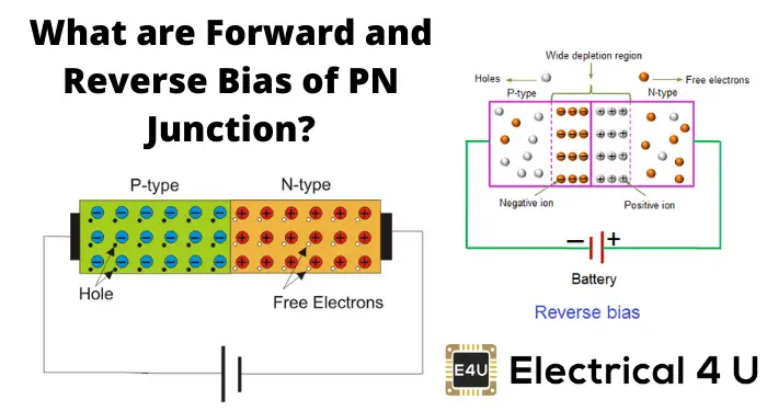
Let's summarize these two states. The diagram below illustrates the behavior of the charge carriers and the depletion region in each case.
-
Forward Bias: When the P-type side (anode) is connected to a more positive voltage than the N-type side (cathode), the external voltage opposes the built-in potential barrier. This shrinks the depletion region. If the forward voltage is sufficient to overcome the barrier (typically ~0.7V for a silicon diode), majority carriers have enough energy to cross the junction, and a significant current flows. The diode acts like a closed switch.
-
Reverse Bias: When the P-type side (anode) is connected to a more negative voltage than the N-type side (cathode), the external voltage adds to the built-in potential. This pulls majority carriers away from the junction, widening the depletion region. The barrier to current flow increases, and almost no current flows (apart from a tiny leakage current due to minority carriers). The diode acts like an open switch.
The Diode's I-V Characteristic Curve
The relationship between the voltage across a diode and the current through it is non-linear and is best described by its I-V (current-voltage) characteristic curve.
PN Junction Diode and Diode Characteristics
This article from Electronics-Tutorials.ws provides a detailed breakdown of the diode's behavior under different bias conditions, culminating in the I-V curve.
Read the section on Reverse Biased PN Junction Diode. Note the explanation of the extremely small leakage current. Next, read the section on Forward Biased PN Junction Diode. Pay attention to the "knee" voltage, the point where current begins to flow rapidly. Finally, look at the diagram in the section Ideal and Real Characteristics. This graph elegantly summarizes everything we've discussed.
The I-V curve reveals two other important practical details:
- Forward Voltage Drop (): In the forward-biased state, even when conducting, there is a relatively constant voltage drop across the diode. For standard silicon diodes, this is about 0.6V to 0.7V.
- Reverse Breakdown Voltage (): If the reverse-bias voltage is increased beyond a certain limit, the diode will abruptly break down and conduct a large current. This is called the avalanche effect and can permanently destroy a standard diode.
The Diode in Simple Circuits
The diode's one-way-street behavior makes it incredibly useful. Let's explore two examples that demonstrate its practical and logical roles.
Application: Rectification and Protection
One of the most common uses for a diode is to convert Alternating Current (AC) into Direct Current (DC), a process called rectification. A single diode can perform half-wave rectification, essentially chopping off the negative half of an AC waveform, ensuring the current only flows in one direction. Another simple but critical use is for reverse polarity protection, where a diode is placed in series with a circuit to prevent damage if a power supply is connected backward.
The "Why We Use Them" section of the article from The Engineering Mindset discusses these applications.
Please read the section Why We Use Them to see how a diode can be used for circuit protection and as a simple rectifier.
Application: Diode Logic
This is where we connect the physics of semiconductors directly back to the digital logic you learned in Module 1. Before the invention of integrated circuits based on transistors, simple logic gates were often constructed using diodes. Given your background in computer science, this should be particularly interesting as it forms a physical basis for logical operations.

Let's analyze these circuits, assuming a "HIGH" voltage is +5V and a "LOW" voltage is 0V (ground).
-
OR Gate (right diagram): The output Q is connected to ground through a resistor R1.
- If both inputs A and B are LOW (0V), no current flows through the diodes, and Q is held LOW by the resistor.
- If either A or B is HIGH (+5V), the corresponding diode becomes forward-biased. Current flows from the HIGH input through the diode and resistor to ground. This creates a voltage drop across R1, pulling the output Q HIGH (to approximately 4.3V, which is 5V minus the 0.7V diode drop).
- Thus, Q is HIGH if A or B is HIGH. This is the definition of an OR gate.
-
AND Gate (left diagram): The output Q is connected to +5V through a resistor R1.
- If both inputs A and B are HIGH (+5V), there is no voltage difference across the diodes, so they do not conduct. No current is drawn away from Q, so the resistor R1 pulls Q HIGH.
- If either A or B is LOW (0V), the corresponding diode becomes forward-biased. Current flows from the +5V supply, through R1, through the forward-biased diode, to the LOW input. This effectively connects Q to ground (through the diode), pulling the output Q LOW (to approximately 0.7V).
- Thus, Q is HIGH only if A and B are HIGH. This is the definition of an AND gate.
This "diode logic" demonstrates a powerful concept: physical devices with specific electrical properties can be arranged to perform logical computations.
Conclusion
In this lesson, you've bridged the gap between doped silicon and a functional electronic component. We've seen how joining P-type and N-type materials creates a PN junction with a built-in potential barrier, giving it the signature one-way current flow property of a diode.
Key takeaways from this lesson include:
- A PN junction forms a depletion region at its interface, which creates a potential barrier.
- Forward biasing a diode (positive to P-side) shrinks the depletion region and allows current to flow once the barrier potential (~0.7V for silicon) is overcome.
- Reverse biasing a diode (negative to P-side) widens the depletion region, blocking current flow.
- The I-V curve graphically represents this non-linear, one-way conduction.
- Diodes are essential for applications like AC-to-DC rectification and can even be used to build primitive logic gates.
You now understand the diode, a two-layer semiconductor device. In our next lesson, we will build upon this by adding a third layer to create a bipolar junction transistor (BJT). You will see how this three-layer structure gives us the ability to use a small current to control a much larger one, enabling the creation of electronic switches and amplifiers—the true building blocks of the digital logic circuits you've studied.
Can't find a good explanation? Sign up and we'll make it for you
Sign up