
Welcome to the second module of our course! In the first module, you mastered the art of designing and simplifying combinational logic circuits. We treated logic gates as ideal black boxes, but as you know from our final lesson on hazards, the real world is more complex. Your goal is to understand how everything connects, from the transistor up, and this module marks a crucial step in that journey. We will now dive deep into the physical foundations of digital electronics.
This lesson begins our exploration by answering a fundamental question: how do we transform a simple element like silicon into the versatile material that powers every computer chip? We will cover the basic principle of semiconductor doping. You'll learn why pure silicon is a poor conductor and how we can intentionally introduce impurities to create two new types of materials—N-type and P-type—which have precisely controlled electrical properties. These two materials are the essential ingredients for building diodes and transistors, the bedrock of all digital logic.
From Insulator to Semiconductor: The Case of Silicon
To understand how a transistor works, we first need to understand the material it's made from: silicon. A silicon atom has four electrons in its outermost shell, called the valence shell. In a pure silicon crystal, each atom forms strong covalent bonds with four neighbors, sharing its valence electrons.
This structure is very stable. All the electrons are tightly bound, leaving none free to move around and carry an electrical current. Consequently, pure silicon is a very poor conductor, much closer to an insulator like glass. To make it useful, we need to find a way to introduce mobile charge carriers. This process is called doping.
The video "How semiconductors work" by Ben Eater provides an excellent, intuitive introduction to this entire concept.
This video visually explains why pure silicon doesn't conduct and how doping with different elements changes its properties to create N-type and P-type materials.
Please watch the entire video from start to finish. As you watch, focus on: Why the covalent bonds in pure silicon prevent electricity from flowing. How adding phosphorus introduces a "free electron." How adding boron creates a "hole" and how this hole can "move." The final, crucial point about why these materials remain electrically neutral.
N-Type and P-Type Doping
As you saw in the video, we can alter silicon's properties by replacing a tiny fraction of silicon atoms with atoms of a different element. There are two key ways to do this.
N-Type Semiconductor (Adding Electrons)
If we introduce an element with five valence electrons, such as Phosphorus (P), into the silicon crystal, something interesting happens. Four of Phosphorus's valence electrons form covalent bonds with the neighboring silicon atoms, fitting perfectly into the crystal structure. However, this leaves one electron leftover. This electron is not part of any bond and is only weakly attached to its original phosphorus atom. It takes very little energy to set it free, allowing it to move throughout the crystal lattice.
Because this process adds a negatively charged mobile carrier (the electron), the resulting material is called N-type semiconductor. The added impurity atom (Phosphorus) is called a donor atom because it "donates" a free electron.
In N-type material, these donated electrons are the primary charge carriers and are called majority carriers. Although rare, thermal energy can still break a covalent bond, creating an electron-hole pair. The holes in N-type material are called minority carriers.

P-Type Semiconductor (Adding "Holes")
Conversely, if we introduce an element with only three valence electrons, such as Boron (B), we get a different effect. When a boron atom replaces a silicon atom in the crystal, it can only form covalent bonds with three of its neighbors. This leaves one bond incomplete, creating a vacancy where an electron should be. This vacancy is called a hole.
A hole has an effective positive charge. A valence electron from a nearby bond can easily jump into the hole, filling it. However, this leaves a new hole in the spot the electron just left. The result is that the hole appears to have moved. This movement of holes through the crystal lattice can sustain an electrical current.
Because this process introduces a positively charged mobile carrier (the hole), the material is called a P-type semiconductor. The impurity atom (Boron) is known as an acceptor atom because it "accepts" an electron from a nearby bond.
In P-type material, holes are the majority carriers. The few free electrons that are created by thermal energy are the minority carriers.
Formalizing the Concepts
The video provided a great intuitive foundation. Now, let's solidify these ideas with some formal definitions and a more detailed look at the underlying atomic physics from the textbook "Electronic Devices" by Thomas Floyd.
[PDF] IntroductIon to SemIconductorS - Higher Education | Pearson
This chapter provides a detailed, foundational explanation of atomic structure and the doping process. It will reinforce what you saw in the video with more formal terminology.
First, quickly read the section The Bohr Model (Section 1-1) to review the concepts of valence electrons and ionization. Next, read the section on materials, focusing on the introduction and the part discussing Covalent Bonds (Section 1-2). This explains silicon's crystal structure. Finally, read the core section for this lesson, N-type and P-type Semiconductors (Section 1-4). This section formally defines N-type and P-type materials, donors, acceptors, and majority/minority carriers.
The key takeaway is that by doping, we create an imbalance between the number of free electrons and holes.
- Intrinsic (pure) silicon: Number of free electrons ≈ Number of holes (both are very low).
- N-type silicon: Number of free electrons >> Number of holes.
- P-type silicon: Number of holes >> Number of free electrons.
The following table provides a concise summary of the differences, which you can use as a quick reference.
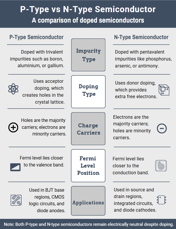
For a deeper dive into the physics, the video below discusses doping from the perspective of energy bands, different types of dopant atoms, and the practical concentrations used in manufacturing.
Doping: The Most Important Part of Making Semiconductors
This video expands on the concepts by introducing energy band diagrams and discussing the practical choice of dopants.
I recommend watching from 04:29 to 09:00. This part covers: How adding phosphorus (N-type dopant) creates a new energy level for the extra electron. How adding boron (P-type dopant) creates a vacancy, or hole, in the valence band. A list of other common dopants from the periodic table and why some are preferred over others.
Conclusion
In this lesson, you've taken the first and most crucial step into the world of semiconductor physics. We've moved from the abstract world of logic gates to the tangible properties of silicon atoms. You now understand how a material that is naturally an insulator can be precisely engineered to conduct electricity.
Here are the key takeaways:
- Pure silicon is a poor conductor because its four valence electrons are locked in stable covalent bonds.
- Doping is the process of adding impurity atoms to a semiconductor to change its electrical properties.
- Doping with a pentavalent element (5 valence electrons) like phosphorus creates N-type material, which has an excess of free electrons (majority carriers).
- Doping with a trivalent element (3 valence electrons) like boron creates P-type material, which has an excess of holes (majority carriers).
- Despite having mobile charge carriers, both N-type and P-type materials are electrically neutral overall.
You now have two distinct types of materials, one with mobile negative charges and one with mobile positive charges. What happens if we join them together? That is the subject of our very next lesson, where we will explore the PN junction. This simple structure is the heart of the diode and the fundamental building block for the transistors that make up the logic gates you're already familiar with.
Can't find a good explanation? Sign up and we'll make it for you
Sign up