
Hello! In our last lesson, you mastered the Karnaugh map, a powerful visual tool for simplifying Boolean functions into their minimal sum-of-products (SOP) form. This is a crucial step in designing efficient digital circuits. Now, we'll take the next logical step: translating those simplified algebraic expressions into actual circuit diagrams.
This lesson bridges the gap between abstract Boolean algebra and concrete hardware implementation. We will explore how to build logic circuits using two different approaches. First, we'll use the basic building blocks you're already familiar with: AND, OR, and NOT gates. Then, we will dive into the concept of universal gates—NAND and NOR—and see how they can be used exclusively to construct any logic function. This is a common practice in real-world integrated circuit (IC) design, and understanding it will bring you one step closer to your goal of seeing "how every dot connects," from the logic expression down to the physical implementation.
From Expression to Circuit: Basic Gates
Once you have a simplified Boolean expression, implementing it with basic gates is a straightforward, mechanical process. A sum-of-products (SOP) expression, like the ones you derived from K-maps, naturally maps to a specific two-level circuit structure:
- A first level of AND gates to create each product term.
- A second level consisting of a single OR gate to sum the outputs of the AND gates.
- Any necessary NOT gates (inverters) to provide the complemented inputs.
Let's consider the expression . We can see it has two product terms ( and ) that are summed together. The circuit would be built as follows:
- An inverter takes input
Ato produce . - One 2-input AND gate takes and
Bas inputs to produce the term . - A second 2-input AND gate takes
BandCas inputs to produce the term . - Finally, a 2-input OR gate takes the outputs of the two AND gates to produce the final output .
This direct translation is the simplest way to visualize a function's structure. However, in practice, digital circuits are often not built this way. For reasons of efficiency and manufacturing simplicity, designers frequently rely on universal gates.
The Power of Universal Gates: NAND and NOR
A universal gate is one from which any other logic function can be constructed. The two universal gates are NAND and NOR. But why would we want to build everything from just one type of gate?
The article "Implementing Logic Functions Using Only NAND or NOR Gates" provides an excellent summary of the historical and practical reasons.
Implementing Logic Functions Using Only NAND or NOR Gates - EEWeb
This article explains the practical motivations behind designing circuits with a single gate type. It connects theoretical exercises to real-world engineering constraints.
Please read the section titled Why use only NAND or NOR gates?. As you read, focus on points 3 and 4, which discuss transistor count and speed.
As the article highlights, NAND and NOR gates are simpler and faster at the physical transistor level. In the next module, we will explore exactly how a CMOS AND gate is typically constructed from a NAND gate followed by an inverter. This use of universal gates is a foundational concept in IC design, as it allows for simpler, more regular, and higher-performance circuits.
Implementing Functions with Only NAND Gates
To build any circuit from NAND gates, we must first be able to replicate the functions of NOT, AND, and OR. The image below shows how this is done.
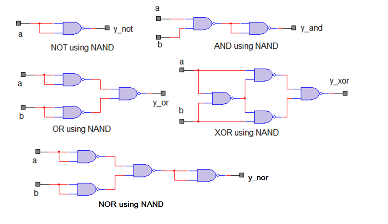
The key to efficiently converting a standard circuit to a NAND-only version lies in the expression's form. For NAND gate implementation, you should start with a Sum-of-Products (SOP) expression.
The process is remarkably elegant. A two-level AND-OR circuit for an SOP expression can be directly converted to a two-level NAND-NAND circuit. This works because of De Morgan's laws. Let's look at .
This final expression is purely in terms of NAND operations. Graphically, this is equivalent to replacing every gate in the two-level AND-OR schematic with a NAND gate.
The following resource provides a systematic method for this conversion.
NOR and NAND Implementation - Two level & Multilevel Implementation
This guide details the step-by-step conversion process from a standard AND-OR circuit to a NAND-only implementation.
First, read the sections Introduction to NAND Gate & Its Implementation and "Two-Level Implementation using NAND Gate." Pay close attention to the "Mixed Notation" concept, where bubbles (inversions) are added and canceled out to transform the circuit. The example for F = A B + B C + D is particularly useful as it shows how to handle a term that isn't part of an AND gate.
Let's walk through a complete example using the insights from the video "NAND/NOR Only Example" by Peter Mathys. The video analyzes the function .
This video provides a worked example showing how an SOP function is implemented first with basic gates and then efficiently with only NAND gates.
First, watch the initial setup from 00:00 to 02:49, where the function is minimized to the SOP expression F = \overline{X_1}X_2 + X_1X_3 and implemented with basic gates. Then, watch the conversion to a NAND-only circuit. Notice how the AND-OR structure transforms directly into a NAND-NAND structure.
As the video demonstrates, the AND-OR implementation and the NAND-NAND implementation for an SOP expression have the same number of gates and are equally efficient.
Implementing Functions with Only NOR Gates
Just as NAND gates are universal, so are NOR gates. We can also create NOT, AND, and OR gates using only NORs. The logic is parallel to the NAND case.
However, there is one crucial difference in the design process. If you try to convert an SOP expression directly into a NOR-only circuit, you often end up with a complicated and inefficient design.
Continuing with the same example, this part of the video demonstrates the inefficiency that results from trying to convert the SOP expression into a NOR-only circuit.
Watch the section from this timestamp. You don't need to follow every detail of the conversion; the key takeaway is to observe how the gate count and complexity increase significantly.
The problem is that NOR gates are naturally suited for a different algebraic form. For efficient NOR gate implementation, you should start with a Product-of-Sums (POS) expression.
Recall from the previous lesson that you can find the SOP form by grouping the 1s in a K-map. To find the POS form, you do the opposite: you group the 0s. Each group of 0s gives you a simplified sum term (an OR term), and the final expression is the product (ANDing) of these terms. A POS expression like has an OR-AND structure, which converts directly to a NOR-NOR structure.
The image below shows a K-map where the 0s are grouped to obtain a POS expression, . It also shows the corresponding OR-AND implementation and the equivalent, efficient NOR-NOR implementation.

Let's return to our video example to see this principle in action. The presenter shows that the most effective way to create a NOR-only circuit is to first find the minimal POS expression for the function.
This final part of the video demonstrates the correct and efficient method for NOR-only implementation by starting with the POS form of the function.
Watch from 07:28 to the end. Pay attention to the logic: The function is re-expressed in POS form by synthesizing the zeros. This POS expression is minimized to F = (X_1+X_2)(\overline{X_1}+X_3). This OR-AND expression is then easily converted to an efficient NOR-NOR circuit with the same low cost as the original NAND implementation.
Conclusion
In this lesson, we have connected the dots from a simplified Boolean expression to a hardware circuit diagram. You now have the tools to implement any combinational logic function you design.
Here are the most important takeaways:
- A Sum-of-Products (SOP) expression maps directly to a two-level AND-OR circuit.
- A Product-of-Sums (POS) expression maps directly to a two-level OR-AND circuit.
- NAND and NOR gates are universal gates, meaning they can be used to build any logic function. This is preferred in practice for efficiency and speed.
- To create an efficient NAND-only circuit, start with an SOP expression. The AND-OR structure converts to a NAND-NAND structure.
- To create an efficient NOR-only circuit, start with a POS expression (derived by grouping zeros in a K-map). The OR-AND structure converts to a NOR-NOR structure.
You are now able to design, simplify, and implement combinational logic circuits from scratch. However, our ideal models sometimes miss real-world effects. In our next and final lesson of this module, we will investigate logic hazards—brief, unwanted output glitches that can occur in these circuits due to signal timing differences—and learn how to design them out.
Can't find a good explanation? Sign up and we'll make it for you
Sign up