
Welcome to the final lesson in our module on Digital Logic Fundamentals. So far, we have treated our logic circuits as ideal, instantaneous systems. You've become proficient at taking a problem, creating a truth table, using a Karnaugh map to find a minimal expression, and finally implementing that expression with logic gates.
However, in the physical world, nothing is instantaneous. Every logic gate takes a small but finite amount of time to react to changes at its inputs. In this lesson, we will explore the consequences of these delays. You will learn how they can cause brief, unwanted glitches in a circuit's output, a phenomenon known as a logic hazard. We will investigate the different types of hazards and, most importantly, learn how to find and eliminate them at the design stage. This will complete your foundational toolkit for designing robust combinational circuits.
The Source of the Problem: Propagation Delay
The idealized logic gates we've used so far change their output state at the exact same moment their input changes. Real gates do not. The time it takes for a change at an input to cause a corresponding change at the output is called propagation delay.
[PDF] Basic Digital Circuits - DiscountPDH
This document provides a good introduction to the non-ideal properties of real logic gates.
Please read the section titled Propagation Delay (page 10). Pay attention to the definitions of t_{PLH} (low-to-high) and t_{PHL} (high-to-low) propagation delay and the fact that these two values are not always equal.
The critical insight is that different paths through a combinational logic circuit will have different cumulative propagation delays. A signal that passes through a single AND gate will arrive at the output faster than a signal that must first pass through an inverter and then an AND gate. This timing difference is the root cause of logic hazards.
What are Logic Hazards?
A hazard is the potential for a temporary, incorrect output value as a circuit's inputs change. This temporary incorrect value is often called a glitch. These glitches occur because, during the input transition, one signal path "wins the race" and changes the output before another, slower path can "correct" it.
Let's formally define the types of hazards.
[PDF] Combinational Logic Design Principles. Combinational Circuits ...
These lecture slides give precise, formal definitions for the different types of hazards and their causes.
First, read the two slides titled Introduction to understand the concept of transient behavior and glitches. Then, read the definitions and view the accompanying timing diagrams for Static-1 Hazard, Static-0 Hazard, and Dynamic Hazards. You can skim the circuit specifics for now; focus on understanding the definition of each hazard from its description and timing diagram.
To summarize the key definitions from the reading:
- Static Hazard: The output is supposed to remain at a constant value, but it momentarily glitches to the opposite state.
- Static-1 Hazard: The output should be steady at
1but temporarily glitches to0. - Static-0 Hazard: The output should be steady at
0but temporarily glitches to1.
- Static-1 Hazard: The output should be steady at
- Dynamic Hazard: The output is supposed to transition from one state to another (e.g.,
0to1) but changes more than once (e.g.,0 -> 1 -> 0 -> 1).
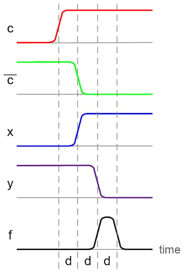
The image below shows a timing diagram for a static-0 hazard. The output f is meant to stay at 0 as other signals change, but due to propagation delays, it briefly spikes to 1.
Analyzing and Fixing Static Hazards
Static hazards are the most common type and can be systematically found and eliminated using the Karnaugh map skills you already possess. Let's walk through an example.
The video "4.5 - Timing Hazards & Glitches" provides an excellent, detailed analysis of how a static-1 hazard occurs in a minimal circuit.
4.5 - Timing Hazards & Glitches
This video demonstrates how a seemingly correct, minimal circuit can produce a glitch. It carefully builds a timing diagram to show exactly why it happens.
First, watch from the beginning to 01:55 to see how the minimal SOP expression F = BC + A\overline{C} is derived from a K-map and implemented as a circuit. Next, watch the detailed timing analysis from 02:01 to 09:33. This is the core of the lesson. The presenter analyzes the transition from input 111 to 110. Follow how the different delays through the two AND gates and the inverter cause the final OR gate's inputs to both be 0 for a brief instant, creating the glitch.
As the video demonstrates, the hazard occurred during the transition between two adjacent cells in the K-map (111 and 110) that were covered by different product terms. For a moment, as the C input changed, the term turned off before the term had time to turn on.
This reveals the rule for fixing static-1 hazards in SOP circuits:
To eliminate static hazards, you must ensure that every pair of adjacent 1s in the K-map is covered by a single product term.
This often requires adding a redundant term that overlaps the existing minimal terms. This redundant term acts as a bridge, holding the output at 1 during the transition when the other terms might momentarily be 0. This results in a "complete sum" of prime implicants, which is not strictly minimal but is robust.
The video "Static Hazards Explained" provides a very clear demonstration of this fix.
This video provides another walkthrough of a static hazard, focusing clearly on the cause and the K-map based solution.
First, watch from the beginning to 07:04. The presenter sets up a similar problem and carefully traces the signal delays to show how the output X momentarily glitches low. Then, watch the solution from 07:04 to the end. Notice how adding a new implicant (BC') on the K-map, which covers the hazardous transition, translates to adding a redundant AND gate to the circuit. This new gate keeps the output high during the transition, eliminating the glitch.
The same principle applies in reverse for static-0 hazards in Product-of-Sums (POS) circuits. To prevent them, you must ensure that every pair of adjacent 0s is covered by a single sum term.
Mitigation Strategies in Practice
We've focused on the design-based fix: adding redundant logic. This is the fundamental way to create a hazard-free combinational circuit. However, in the context of larger digital systems, there are other approaches.
4.5 - Timing Hazards & Glitches
This final part of the video on timing hazards summarizes the different ways designers deal with glitches.
Please watch from 10:26 to the end. The video discusses three methods: Wait: Calculate the worst-case delay and only sample the output after it's guaranteed to be stable. Match Delays: Try to make all signal paths have the same delay. Insert Logic: The redundant term method we just studied.
As the video explains, trying to perfectly match delays is impractical. The most common approach in modern digital design, especially in the microcontrollers and complex ICs you're interested in, is the first one: waiting.
These systems are typically synchronous, meaning their operations are coordinated by a master clock signal. The output of a block of combinational logic is only "read" or stored on a specific edge of the clock. The clock's frequency is chosen to be slow enough to allow all glitches to die out and the outputs to settle to their final, correct values before they are sampled. We will explore synchronous design in great detail when we get to sequential logic. For now, it's important to understand both the cause of hazards and the fundamental design technique to eliminate them.
Conclusion
This lesson completes your journey through the fundamentals of combinational logic design. You now understand not only how to create an ideal circuit, but also how to account for real-world imperfections to make it robust.
Key takeaways from this lesson:
- Real logic gates have propagation delays, which are the root cause of logic hazards.
- A static hazard is a momentary glitch in an output that should be stable (
1 -> 0 -> 1or0 -> 1 -> 0). - A dynamic hazard involves multiple transitions when only one is expected (
0 -> 1 -> 0 -> 1). - Static hazards in SOP circuits can be found on a K-map by looking for adjacent 1s that are not covered by a common term.
- The fix is to add a redundant logic term that covers the hazardous transition, creating a hazard-free but non-minimal circuit.
- In practice, many modern synchronous systems handle hazards by using a clock to wait for outputs to become stable before sampling them.
With this module complete, you have a solid grasp of how to specify, simplify, and implement combinational logic functions. You've connected the dots from a Boolean expression to a hardware diagram. In the next module, we will dive one level deeper in our bottom-up exploration. We'll ask: what are these logic gates actually made of? We will begin our study of semiconductor physics and see how transistors are used to build the logic gates that serve as the foundation of all digital electronics.
Can't find a good explanation? Sign up and we'll make it for you
Sign up