
Welcome. This module moves from the Linux workstation into the hardware beneath the software stack: the AM62x application processor, its attached memories, and the peripherals that later become Linux devices, device-tree nodes, and drivers.
For an automotive or industrial gateway, a block diagram is not merely documentation. It is the first tool for answering practical questions: Which processor runs Linux? Where can early boot code execute before DRAM works? Which interface reaches the Ethernet PHY or CAN controller? Which components are external chips rather than functions inside the SoC? This lesson develops a disciplined way to answer those questions without assuming that a drawing reveals more than it actually does.
Read diagrams at the correct level of abstraction
A hardware diagram can describe several different things. Confusing them leads to incorrect design decisions.
| Diagram type | What it answers well | What it usually does not answer |
|---|---|---|
| SoC functional diagram | Processor cores, hardware accelerators, internal SRAM, controllers, high-level interconnect | Exact register addresses, board connectors, electrical details |
| Board or system-on-module block diagram | How SoC interfaces reach DDR, storage, PHYs, codecs, connectors, PMICs, and external ICs | Internal AM62x bus topology and precise peripheral register addresses |
| Memory map | Which physical address ranges correspond to RAM, SRAM, ROM, or peripheral register windows | PCB wiring and connector pinouts |
| Schematic | Pins, voltage rails, pull resistors, level shifters, clock sources, and electrical connections | Software ownership and bootloader memory allocation |
The supplied VAR-SOM-AM62x diagram is a system-on-module connectivity diagram. It places the AM62x at the center and shows which SoC interfaces leave the module through the SO-DIMM connector or reach on-module memories and support devices. It is not a complete internal AM62x block diagram and it does not provide a register-level memory map.
AM62x SK Evaluation Modules User's Guide (Rev. D)
Read the relevant overview and interface-mapping material from Texas Instruments. It establishes the AM62x processing resources and gives a concrete example of how named SoC interfaces connect to real board devices.
Start with the Description on p. 1, then read Section 1.1, “Introduction” (p. 4), and the memory subsection of Section 2.1.1, “Key Features” (p. 6). Focus on the relationship among the AM62x, external DDR4, eMMC, OSPI flash, and removable SD storage; use the memory list as a landmark. Next, inspect Figures 2-3 through 2-6 in Sections 2.1.2 and 2.1.3 (pp. 8–11). These are board-level functional block diagrams: distinguish the SoC-facing interface names from the physical parts and connectors attached to them. Then read Table 2-1, “AM62x SKEVM Interface Mapping,” in Section 2.1.4 (p. 12), using the interface table to connect each external device to its named SoC port.
The key AM62x processing resources identified in TI’s guide are:
- A quad-core 64-bit Arm Cortex-A53 application processor subsystem. This is the processor class that normally runs U-Boot and Linux.
- A Cortex-R5F microcontroller core in the MCU domain. On K3-family devices, this domain has an important role in the early boot architecture.
- A Cortex-M4F microcontroller core for firmware-oriented tasks.
- On relevant AM62x variants and boards, PRU-SS programmable real-time I/O resources, which are distinct from the A53 Linux application cores.
Do not treat every programmable engine as interchangeable. A quad A53 subsystem is designed for a rich OS, virtual memory, and application workloads. An R5F, M4F, or PRU subsystem is generally used for deterministic control, firmware, device management, or specialized I/O work. The exact software partitioning is a product architecture decision, but the block diagram tells you the available execution domains.
First pass: classify everything in the VAR-SOM-AM62x diagram
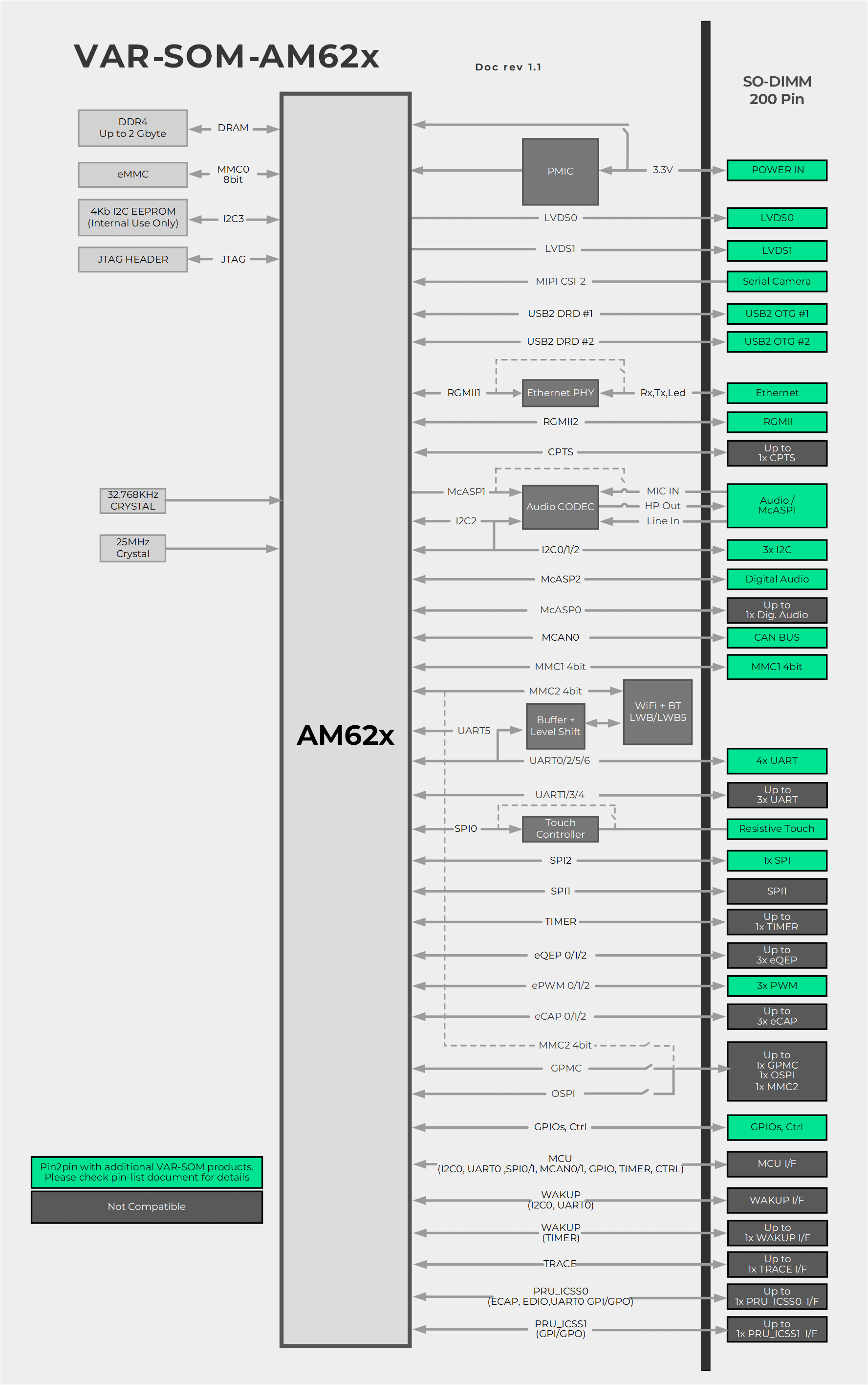
Use a four-part classification on every block:
- Compute resource: executes instructions.
- Memory resource: holds instructions or data.
- Controller or peripheral: provides a hardware function exposed through registers.
- External device or connector: sits outside the SoC and communicates through a controller and physical interface.
Applied to the supplied diagram:
| Diagram element | Classification | Interpretation |
|---|---|---|
| AM62x | SoC containing compute, interconnect, memory-controller, and peripheral-controller resources | The central silicon device; individual controllers inside it are not separately drawn. |
| DDR4, up to 2 GB | External volatile main memory | Connected through the SoC’s DDR controller and PHY. Linux code, page tables, kernel data, applications, DMA buffers, and filesystem cache ultimately reside here. |
| eMMC, MMC0 8-bit | External nonvolatile managed flash storage | A storage device accessed through the AM62x MMC controller. Its contents are not ordinary byte-addressed CPU RAM. |
| 4-kbit I2C EEPROM | External nonvolatile support memory | Often used for module identification or board data; in this diagram it is marked for internal use. |
| PMIC | External power-management peripheral | Supplies and sequences rails needed by the SoC and board. It is commonly configured through I2C or similar control paths. |
| Ethernet PHY | External physical-layer device | Converts the AM62x Ethernet controller’s digital MAC-side interface, such as RGMII, into electrical Ethernet signaling. |
| Audio codec | External mixed-signal peripheral | Converts digital audio streams from McASP into analog microphone, line, and headphone signals. |
| Wi-Fi and Bluetooth module | External communications subsystem | Connected through controller interfaces such as MMC, UART, and audio paths, with any needed level shifting or buffering. |
| SO-DIMM 200-pin connector | Module boundary and electrical interconnect | It is not a peripheral itself. It exports AM62x signals to a carrier board. |
This classification avoids a common error: calling eMMC, an Ethernet PHY, or a connector “memory-mapped.” Usually, the controller registers inside the SoC are memory-mapped. The external device is then reached through its protocol.
For example:
- Software writes the AM62x MMC controller’s register window.
- The controller sends commands and data over the MMC bus to eMMC.
- eMMC performs internal flash management and returns data, often with DMA transferring payload data into DDR.
The CPU does not normally load an arbitrary eMMC byte using the same mechanism used to load a variable from DDR. Similarly, software configures an Ethernet controller through registers; the controller and DMA machinery move frames between DDR and the external PHY over RGMII.
The SoC is a network, not a collection of direct wires
A modern application processor has multiple bus masters and bus slaves.
- A master initiates a transaction. A CPU core, DMA engine, display engine, or Ethernet controller can act as a master.
- A slave responds to an addressed transaction. DDR memory, on-chip SRAM, and a peripheral register bank are typical slaves.
- The interconnect or bus fabric transports requests, decodes addresses, arbitrates competing requests, and applies access controls.
At a conceptual level, an A53 core does not have one dedicated wire to DDR, another to UART, and another to Ethernet. It issues transactions into an on-chip fabric. The transaction’s address determines whether the fabric routes it to DRAM, SRAM, or a peripheral register window.
A useful mental model is:
| Addressed destination | Typical result of an A53 access |
|---|---|
| DRAM address | Reads or writes ordinary program data, stacks, heap objects, page tables, or DMA buffers |
| On-chip SRAM address | Reads or writes fast internal memory, especially useful before external DRAM is usable |
| Peripheral register address | Configures hardware, checks status, acknowledges interrupts, or transfers small control data |
| Invalid or protected address | Raises an abort or bus error, or is blocked by a firewall/access-control mechanism |
The fabric matters directly to gateway design. Ethernet, USB, display, camera, storage, and accelerator controllers can need high-bandwidth access to DDR at the same time as the A53 cluster runs Linux. This is why a block diagram may show a peripheral apparently “connected” to the AM62x but not show its actual data path: much of the traffic travels internally between the peripheral’s DMA engine and DRAM.
A peripheral’s control path and its bulk-data path are therefore often different:
- Control path: CPU writes configuration registers, reads status, and services error conditions.
- Bulk-data path: DMA transfers packet payloads, storage blocks, audio samples, or video buffers between the peripheral and DDR.
For a CAN gateway, the data volumes are modest compared with video, but the distinction remains important. Linux configures the CAN controller through its register interface, while received frames are delivered through controller-managed buffers and the networking stack. The external CAN transceiver is yet another component, translating controller-level logic signals to the physical CAN bus.
SRAM, DRAM, and persistent storage serve different boot-time roles
The memory names in a diagram encode important physical constraints.
On-chip SRAM
Static RAM (SRAM) is integrated into the SoC. It is relatively small, fast, and available immediately after reset once the relevant power and clock domains are active. It does not require the external DDR interface to be trained first.
That makes SRAM the essential workspace for the earliest code:
- Boot ROM execution support
- A first-stage bootloader
- An initial stack
- A small heap and global-data area
- DDR-controller and DDR-PHY initialization code
- Data structures passed from ROM to early firmware
SRAM capacity is a hard design constraint. In early boot, a large debug print buffer, decompressor, device tree, or driver framework can be enough to exhaust the available space.
External DRAM
DDR4 DRAM is much larger and is the system’s working memory after initialization. But it is external to the AM62x and cannot simply be assumed ready at reset. The processor must first establish suitable clocks and power, configure the controller and PHY, and complete the DDR initialization procedure appropriate to the board’s electrical design.
Only after that can a bootloader safely load large images and eventually launch Linux.
Nonvolatile storage
eMMC, SD, and OSPI flash persist across power loss. They store boot artifacts and filesystems, but their access is mediated through controllers and protocols. They are not a replacement for executable DRAM during normal Linux operation.
This gives the fundamental early-boot constraint:
Persistent storage can contain the next boot image, but SRAM is the initial execution workspace; DRAM becomes the large execution workspace only after successful initialization.
The next lesson will examine the reset-to-DRAM sequence in detail. For now, recognize that SRAM and DRAM occupy different places in both the physical design and the boot story.
Memory maps: addresses are the software view of hardware
A block diagram tells you what exists. A memory map tells you where software reaches it.
A physical address map partitions processor-visible address space into regions. A simplified, conceptual layout might contain:
| Region category | Typical contents | How software uses it |
|---|---|---|
| Boot ROM | Immutable vendor code | Executed immediately after reset |
| Internal SRAM | Early code and temporary runtime data | Used before DDR initialization |
| Peripheral windows | UART, I2C, MMC, Ethernet, GPIO, timer, interrupt-controller registers | Read and written to control hardware |
| External DRAM | Kernel, applications, stacks, heap, page cache, DMA buffers | Main working memory after DDR initialization |
| Reserved or secure regions | Firmware-owned, protected, or unavailable ranges | Must not be overwritten by general-purpose software |
The exact addresses are SoC-, board-, firmware-, and configuration-dependent. Never invent them from a connectivity diagram.
The TI SDK documentation provides two useful examples. The first is a U-Boot R5 SPL SRAM layout. The second is a U-Boot report showing usable DRAM after initialization.
3.1.1.1. General Information — Processor SDK AM62x Documentation
Read TI’s boot-flow context and two memory-layout examples. The aim is not to memorize addresses, but to learn how an early bootloader allocates scarce SRAM before relocating into DRAM.
First inspect Section 3.1.1.1.3, “Boot Flow.” Read the diagram from the ROM and R5 stage through the point where the A53 runs later boot firmware. Use it only to identify the participating execution domains; the detailed boot sequence is the next lesson. Then read all of Section 3.1.1.1.7, “SRAM memory Layout during R5 SPL bootloader stage.” Treat the boxed layout as an allocation map, not as the entire AM62x physical-address map. Identify the separate regions for the SPL image, BSS, ROM boot parameters, stack, global data, and heap. Finally, read Section 3.1.1.1.5, “Available RAM for image download,” beginning with the bdinfo example. Notice that DRAM begins at 0x80000000 in this example, while U-Boot itself reserves high memory for relocation and stack use.
Reading the R5 SPL SRAM layout
The TI layout shows two visible address areas used during early R5 SPL execution:
- At
0x43c00000, the SPL image is placed, followed by reserved space, BSS, device-management configuration data, and ROM-provided boot information. - At
0x70000000, the layout places the stack, global data, and heap.
Several important deductions follow:
-
An address range is not necessarily one uninterrupted resource.
The map has separate allocations and intentionally empty gaps. Gaps may support alignment, ROM contracts, safety margins, or later allocations. -
BSS still consumes memory.
BSS is the zero-initialized storage for global and static variables. It may not enlarge the stored image in the same way as initialized data, but it absolutely consumes SRAM after startup code clears it. -
The stack grows downward.
The TI documentation explicitly notes this for the U-Boot stack. A map must leave room in the growth direction; otherwise a deep call chain or large local object corrupts neighboring memory. -
Boot-ROM data is part of the contract.
The ROM boot parameter table must not be overwritten casually. Early firmware has to preserve or consume it according to the platform’s boot protocol. -
This is not Linux RAM yet.
This layout belongs to the constrained R5 SPL stage. It is not a representation of where Linux will put processes, page cache, or drivers after the A53 starts.
The bdinfo example then shows DRAM beginning at 0x80000000. Once DRAM works, U-Boot can relocate near the high end of available RAM and reserve space for itself and its stack. This is why a boot command that loads a kernel, DTB, and initramfs must use carefully chosen DRAM addresses. Address overlap is not a minor bug: it can overwrite an image that has not yet been booted.
Memory-mapped I/O: registers appear at addresses
A peripheral generally contains a small bank of registers, commonly including:
- Configuration or control registers to enable the peripheral, select modes, configure bitrate or pin behavior, and start operations.
- Status registers to report completion, errors, FIFO state, link status, or interrupt causes.
- Data registers or FIFOs for small transfers.
- Interrupt-enable and interrupt-status registers to control asynchronous notification.
Memory-mapped I/O, abbreviated MMIO, gives those registers physical addresses within the processor’s address space. The CPU accesses them with normal load and store instructions, while the bus fabric routes the operation to peripheral hardware rather than RAM.
Watch “Lecture 5: Memory Mapped I/O” from the Embedded Systems and Deep Learning channel for a concise hardware-level explanation of why peripheral registers occupy address ranges and how a register block is organized.
Watch the definition to establish the distinction between peripheral register locations and special I/O instructions. Then watch the GPIO example. The STM32 addresses are examples only; focus on the transferable ideas of base address, register offset, register width, read-modify-write behavior, and why register declarations use volatile.
Suppose a hypothetical controller has base address , and its status register is at offset . Its physical register address is:
A hardware manual will define:
- the base address ,
- the size of the register window,
- the register offsets,
- the meaning of each bit,
- reset values,
- which bits are read-only, write-only, read-clear, or write-one-to-clear.
That last point is operationally important. Registers are not ordinary C variables. A read can acknowledge an event; a write of 1 can clear a fault bit; a read-modify-write operation can be unsafe if hardware changes the register between the read and write. Correct drivers follow the register semantics defined by the SoC reference manual.
In bare-metal C, a register is often represented using a volatile pointer or a structure whose members correspond to documented offsets. volatile tells the compiler that the value can change independently of program flow and that reads and writes must be emitted rather than optimized away.
Linux adds another layer of discipline:
- A device tree describes the peripheral’s physical register region using a
regproperty. - The kernel driver maps that region with appropriate device-memory attributes.
- Kernel code uses MMIO accessors rather than treating a physical address as an ordinary userspace pointer.
- Applications normally use system calls, device files, sockets, or framework APIs. They do not directly dereference peripheral addresses.
This prevents a userspace process from accidentally reprogramming an MMC controller, GPIO block, or Ethernet MAC.
Trace interfaces in the AM62x diagram without overclaiming
The right side of the VAR-SOM diagram lists interface names. Those labels are strong evidence of the controller path, but not of every internal implementation detail.
Here is how to interpret several representative paths.
DDR4 through DDR0
DDR0 denotes the SoC’s external DDR interface. The central AM62x includes the memory-controller and physical-interface logic; the actual DDR4 chips are external on the module.
Software implication: DDR initialization configures the controller and PHY so that the A53 subsystem can use external RAM. Board implication: routing, termination, reference voltage, and timing are critical even though the diagram reduces the connection to one line.
eMMC through MMC0
MMC0 is an SoC multimedia-card controller interface connected to the eMMC device. The “8-bit” label indicates the bus width shown for that connection.
Software implication: the MMC controller’s registers are MMIO, while the eMMC storage contents are accessed through MMC commands and DMA transfers. This is a likely boot-media path and later may hold boot partitions, a root filesystem, update slots, and persistent data.
Ethernet through RGMII and a PHY
RGMII1 and RGMII2 connect AM62x Ethernet MACs to external Ethernet PHYs. The PHYs then connect to the RJ45 or carrier-board Ethernet hardware.
Software implication: several components are involved when Ethernet fails:
- the MAC controller and its clock/reset configuration,
- pin multiplexing for the RGMII signals,
- PHY reset and power,
- PHY management communication,
- the physical Ethernet link,
- Linux network-driver configuration.
The diagram helps you localize the failure domain. If no PHY exists or its reset line is held low, tuning an IP address in Linux will not produce a link.
CAN through MCAN
The diagram exposes an MCAN interface at the connector. The controller is inside the AM62x. A production carrier board still needs an appropriate CAN or CAN-FD transceiver between logic-level controller signals and the differential vehicle or industrial CAN bus.
For the eventual gateway, this distinction is essential:
| Layer | Typical responsibility |
|---|---|
| AM62x MCAN controller | CAN protocol engine, message RAM, filtering, timing registers, interrupts |
| Carrier-board transceiver | Differential electrical signaling, bus fault behavior, physical CAN connection |
| Linux SocketCAN stack | Network interface abstraction, frame routing, diagnostics, application APIs |
A connector label alone does not prove that a complete CAN physical interface is present. Always confirm the carrier-board schematic, transceiver type, termination strategy, and voltage-domain compatibility.
I2C, SPI, UART, GPIO, and PWM
These interfaces are low-to-moderate-bandwidth control and expansion paths.
- I2C commonly reaches PMICs, EEPROMs, sensors, expanders, and codecs.
- SPI commonly reaches display controllers, ADCs, secure elements, or external flash.
- UART commonly provides boot recovery, console, debug, or modem communication.
- GPIO provides discrete control and status signals.
- PWM provides timed output waveforms, often for control or dimming applications.
The SoC controller registers are memory-mapped. The signals themselves leave the chip through multiplexed pads whose selected electrical function is configured separately. That pin configuration will later appear in device-tree pin-control entries.
A repeatable annotation method
When you receive an unfamiliar SoC, SOM, or carrier-board diagram, create an engineering note with these five sections.
1. State the diagram’s scope
Write one sentence such as:
This is a VAR-SOM-AM62x module-connectivity diagram; it identifies SoC-facing interfaces and external devices but does not define the AM62x internal interconnect or register addresses.
This protects the rest of the analysis from unsupported conclusions.
2. Make a resource inventory
Group visible elements into:
- application CPU subsystem,
- real-time or MCU cores,
- SRAM and external DRAM,
- persistent storage,
- communications controllers and external PHYs or transceivers,
- media and human-machine interfaces,
- power, clocks, reset, debug, and expansion.
3. Record each interface as a chain
For every critical product function, write the entire chain in words. For example:
Linux Ethernet driver, AM62x Ethernet MAC register block, DMA buffers in DDR, RGMII interface, external Ethernet PHY, magnetics and RJ45 on carrier board, physical network.
This style identifies where to look when an interface fails.
4. Separate addressable resources from external protocol devices
Mark the following distinctly:
- MMIO register window: directly addressed by processor transactions.
- RAM: normal memory transactions.
- Protocol-attached device: eMMC, PHY, codec, sensor, or EEPROM reached through a controller.
- Connector: electrical boundary that may expose any of the above.
5. Record unknowns explicitly
Examples of valid unknowns include:
- Exact AM62x register base address for a controller
- Which pins carry a named peripheral interface
- Whether a carrier board adds a CAN-FD transceiver
- Which boot source is selected by straps
- Whether a given device is powered, reset, and clocked in a particular board revision
Those are not shortcomings in your analysis. They are requirements for the next document: the SoC technical reference manual, schematic, pinmux data, device tree, or boot configuration.
Key takeaways
An application-processor block diagram must be read at its intended abstraction level. In the AM62x context:
- The A53 subsystem is the main application-processing resource, while R5F and M4F are distinct MCU-class execution domains.
- SRAM is small, internal, and vital before DDR works; DDR4 becomes the large main memory after initialization.
- eMMC, OSPI, SD, PHYs, codecs, PMICs, and connectors are not interchangeable with CPU-addressable DRAM.
- A bus fabric connects CPU and DMA masters to DRAM and peripheral register windows; peripheral data movement often uses DMA into DDR.
- MMIO means controller registers occupy physical address ranges and are accessed with loads and stores under carefully defined register semantics.
- An early-boot SRAM layout is an allocation contract, while U-Boot’s DRAM report tells you where large boot artifacts can safely reside after DDR initialization.
Next, you will turn this static topology into a reset-to-DRAM sequence: bootstrap configuration is sampled, Boot ROM starts from a constrained environment, clocks and power domains become available, and the bootloader brings external DDR online.
Can't find a good explanation? Sign up and we'll make it for you
Sign up