Hello Alex,
Welcome to the course! I'm excited to guide you through the fascinating world of radioelectronics, building upon your foundational knowledge and diving deep into the principles that power modern technology.
This first module of our journey into active components focuses on the transistor, arguably the most important invention of the 20th century. We'll begin with the Bipolar Junction Transistor (BJT), a device that's fundamental to amplification and switching.
This lesson will cover the BJT's internal structure and the physical principles that govern its operation. Understanding this is essential for analyzing and designing the amplifier and logic circuits we'll explore later.
Approximate time to complete: 45-50 minutes.
1. From Passive to Active: Introducing the Transistor
In the previous modules (which you've mastered through your university studies), you focused on passive components like resistors, capacitors, and inductors. They are essential, but they can only dissipate or store energy. To amplify a signal or to perform logic operations, we need active components. The transistor is the quintessential active component.
A Bipolar Junction Transistor (BJT) is a three-terminal semiconductor device that can function as either a current-controlled switch or an amplifier. A small current flowing into one terminal (the Base) can control a much larger current flowing between the other two terminals (the Collector and Emitter).
To get a practical feel for what this means, let's start with a couple of short video segments.
First, watch this demonstration from The Engineering Mindset. It provides an excellent, high-level overview of what a transistor does in a circuit.
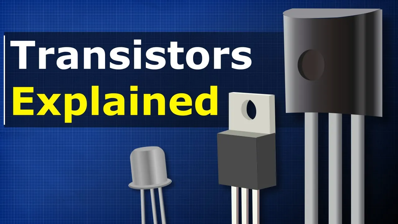
Focus on these two parts:
- Introduction to Transistors (0:00 - 2:06): This introduces the basic function and physical appearance.
- Transistor as a Switch and Amplifier (2:06 - 5:02): This part vividly demonstrates how a small base voltage/current controls a larger circuit, illustrating the core concepts of switching and amplification.
Next, watch this segment for a more formal introduction to the BJT's structure.
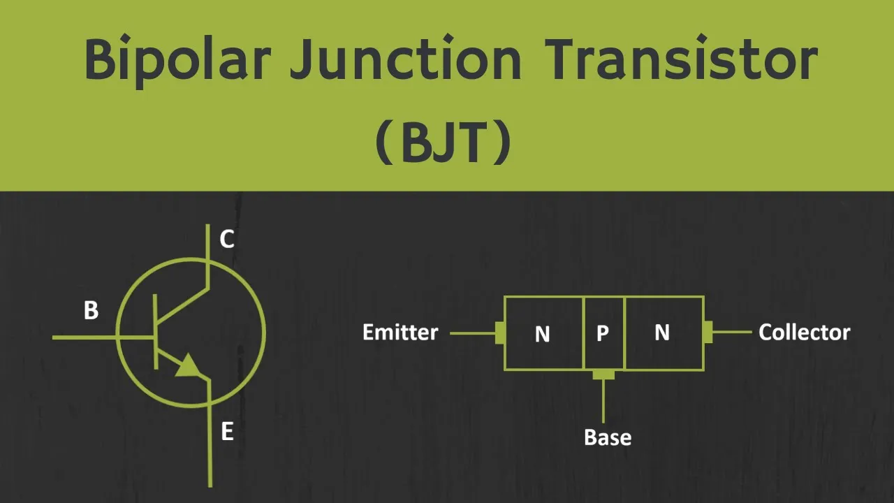
- Introduction to BJT and its Types (0:12 - 1:59): This introduces the NPN and PNP types and explains the meaning of "bipolar"—that both electrons and holes are involved in the current flow.
The key takeaway is that a transistor gives us control. Unlike a simple switch that requires manual operation, a transistor allows a small electrical signal to control a much more powerful one, forming the basis of everything from a radio amplifier to a computer's logic gate.
2. The Inner Workings: Structure and Doping
So, how does a transistor achieve this control? The magic lies in its specific internal construction. A BJT is formed by sandwiching three layers of doped semiconductor material. This creates two main types:
- NPN: A P-type layer is sandwiched between two N-type layers.
- PNP: An N-type layer is sandwiched between two P-type layers.
The three layers are named the Emitter, Base, and Collector. Their physical and electrical properties are deliberately asymmetrical, which is critical to the transistor's function.
Let's examine the specific characteristics of each region. The following video segment explains this concisely.
- BJT Internal Construction and Doping (2:28 - 3:27): Pay close attention to the differences in doping concentration and physical width.
To summarize the crucial points:
- Emitter: Heavily doped. Its job is to emit (or inject) a large number of charge carriers (electrons in an NPN, holes in a PNP) into the base.
- Base: Very thin and lightly doped. This is the key to the transistor's operation. Its thinness ensures most carriers from the emitter can pass right through it, and its light doping minimizes how many of those carriers are "lost" to recombination within the base.
- Collector: Moderately doped and physically the largest. Its job is to collect the vast majority of charge carriers that have traveled from the emitter and through the base. Its larger size helps it dissipate the heat generated by the current flowing through it.
Think of it as a starting line (Emitter), a very narrow checkpoint (Base), and a finish line (Collector). The design ensures most runners who start make it all the way to the end, with only a few getting stopped at the checkpoint.
3. Controlling the Flow: Biasing and Modes of Operation
A BJT has two P-N junctions: the Base-Emitter (BE) junction and the Base-Collector (BC) junction. By applying external voltages to forward- or reverse-bias these junctions, we can place the transistor into one of three main operating regions.
| Operating Region | Base-Emitter Junction | Base-Collector Junction | Primary Application |
|---|---|---|---|
| Cut-off | Reverse-biased | Reverse-biased | Switch (OFF) |
| Active | Forward-biased | Reverse-biased | Amplifier |
| Saturation | Forward-biased | Forward-biased | Switch (ON) |
The following video segment provides a clear walkthrough of these biasing conditions.
- BJT Operating Regions and Biasing (3:14 - 6:21): This covers the voltage conditions required for each region in both NPN and PNP transistors.
Understanding these regions is fundamental. When used in digital logic, a transistor rapidly switches between Cut-off (0) and Saturation (1). When used as an amplifier, it is carefully biased to operate within the Active region.
4. The Active Region in Detail: How Amplification Works
Let's now focus on the Active Region, as this is where the BJT's amplifying properties come to life. We will use an NPN transistor as our example.
In the active region:
- The Base-Emitter junction is forward-biased.
- The Base-Collector junction is reverse-biased.
This specific biasing arrangement is what enables a small base current to control a large collector current.
To see this process in action, please watch the following detailed explanation. This is the most important part of the lesson, as it connects all the concepts we've discussed.
- Working of NPN BJT in Active Region (7:42 - 16:06): This is a fantastic, step-by-step walkthrough of the electron flow, recombination in the base, and the resulting current relationships.
Here is a summary of the key physical processes and resulting mathematical relationships:
- Injection: The forward-biased BE junction causes the heavily-doped emitter to inject a massive flow of electrons into the thin, lightly-doped base. This constitutes the emitter current ().
- Recombination: As these electrons travel through the base, a very small fraction (~1-2%) recombine with the holes present in the P-type base material. This small flow of charge constitutes the base current ().
- Collection: Because the base is so thin and the collector is reverse-biased (and thus has a strong positive potential relative to the base), the vast majority of electrons injected from the emitter are swept across the BC junction and collected by the collector. This large flow constitutes the collector current ().
This leads to the fundamental current relationship in a BJT:
Since is very small compared to , we can see that .
The relationship between the collector current and the base current is defined by the DC current gain, or beta ():
Beta is a measure of the transistor's amplification capability. Typical values range from 50 to 400, meaning a tiny base current of 1 mA could control a collector current of 50-400 mA. This is why the BJT is often described as a current-controlled current source.
Another important parameter is alpha (), which relates the collector current to the emitter current:
Since is just slightly less than , is always slightly less than 1 (typically 0.98 to 0.998).
You can relate the two gain parameters with the following formula, which is a useful exercise to derive yourself from the equations above:
Conclusion
In this lesson, you've revisited the fundamental principles of the Bipolar Junction Transistor. We've established the critical link between its physical structure and its electrical behavior.
Here are the key takeaways:
- A BJT is a three-layer semiconductor device (NPN or PNP) with three terminals: Emitter, Base, and Collector.
- The asymmetric doping and sizing of these regions are essential for its function: a heavily doped emitter, a very thin and lightly doped base, and a large, moderately doped collector.
- By controlling the biasing of the two internal PN junctions, the BJT can operate in three primary modes: Cut-off (off switch), Saturation (on switch), and Active (amplifier).
- In the active region, a small base current () controls a much larger collector current (), a relationship quantified by the current gain, .
- The fundamental current equation is .
You now have a solid foundation for understanding how transistors work.
In our next lesson, we will explore the practical application of these principles by examining the three main BJT Amplifier Configurations: Common-Emitter, Common-Collector, and Common-Base. We'll see how connecting the same device in different ways produces amplifiers with vastly different characteristics in terms of voltage gain, current gain, and impedance.