
Hello, and welcome to the course. Semiconductor metrology only makes sense in the context of what a fab is trying to build: a wafer is progressively transformed from an ultra-flat silicon substrate into many electrically functional dies, then into packaged products. This first module builds that shared manufacturing map before we begin locating the points at which measurements and inspections control it.
In this lesson, you will trace the major manufacturing stages from silicon ingot and wafer preparation through transistor formation, wiring, wafer test, assembly, and advanced packaging. The goal is not to memorize a universal recipe—there is no single one—but to understand the recurring logic of fabrication and where each broad stage fits.
The map: a wafer is built layer by layer
Start with this concise visual overview from Samsung Semiconductor Newsroom, “Semiconductor Manufacturing Process” Explained. It introduces the major stages in the conventional wafer-fabrication and assembly flow. Treat its ordering as a useful map, while remembering that actual products add many specialized steps and repeat the central patterning cycle many times.
‘Semiconductor Manufacturing Process’ Explained | 'All About Semiconductor' by Samsung Semiconductor
Watch Samsung Semiconductor Newsroom’s “Semiconductor Manufacturing Process” Explained for a fast end-to-end view of how a wafer becomes a packaged chip.
Watch the overview and wafer to establish the process vocabulary and see how silicon becomes a polished substrate. Then watch the fabrication cycle, focusing on the distinct purposes of oxidation, lithography, etch, deposition, and ion implantation. Finish with wiring to packaging to connect metal interconnect, electrical die sorting, assembly, and final test.
The central idea is controlled addition, selective removal, and modification of material, carried out with extreme positional and dimensional control. A circuit is not printed in one action. Instead, the fab makes one layer or feature, cleans and checks the wafer, then performs related operations again for the next layer.

The “repeat” loop in the second illustration is more important than the particular number of boxes. Logic and memory devices contain many patterned layers; advanced three-dimensional memory can contain far more. A finished wafer therefore embodies a long history of material deposits, pattern transfers, etches, thermal treatments, cleans, and measurements.
One caution: diagrams often show the main operations as a tidy circle. In practice, the exact sequence changes with the device architecture and layer. For example, an implant may follow a particular lithography-and-etch sequence for one transistor feature, while another layer may involve deposition, planarization, and lithography without any implant. The durable mental model is a controlled, repeated layer-building cycle, not a single fixed twelve-step recipe.
1. Preparing the silicon starting surface
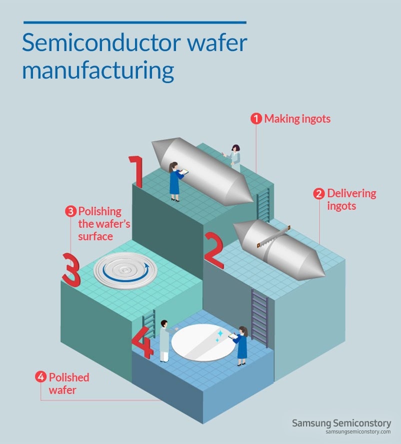
Manufacturing begins with extraordinarily pure silicon. Silicon is refined, melted, and crystallized into a cylindrical single-crystal ingot. A single crystal matters because the orderly atomic lattice gives electronic devices reproducible electrical behavior.
The ingot is sliced into thin circular wafers. These slices do not initially have the flatness, smoothness, thickness uniformity, or cleanliness needed for nanometre-scale patterning. They are processed through operations such as edge shaping, grinding, chemical treatment, and chemical-mechanical polishing. The outcome is a highly flat, mirror-like surface.
Many leading-edge fabs use 300 mm wafers. A larger wafer can hold more dies, but it also increases the engineering challenge: thickness, flatness, temperature, particle contamination, and film uniformity must be controlled across a much larger area.
Before devices are formed, the wafer may receive additional foundational layers:
- Epitaxy can grow a carefully controlled crystalline silicon layer on the wafer.
- Thermal oxidation can form silicon dioxide, which can serve as an insulating, protective, or process layer.
- Initial deposition can place a dielectric, semiconductor, or conductive film on the wafer.
At this stage, the wafer is a prepared substrate, not yet a useful integrated circuit. Its value lies in providing a uniform starting condition for every later process.
2. The repeating pattern-transfer cycle
The following account from ASML, “6 crucial steps in semiconductor manufacturing,” gives a compact explanation of the material-and-patterning stages. Read it to connect the broad map to the physical role of each operation.
6 crucial steps in semiconductor manufacturing
Read ASML’s overview for a focused explanation of deposition, lithography, etch, ion implantation, and the transition to packaging.
In the “Deposition” section, read the wafer and deposition introduction. Focus on why a thin film is added before it can be patterned. Next, in the “Lithography” section, read the lithography explanation. Follow the roles of the reticle, optics, resist, and chemical change in transferring a design onto the wafer. In the “Etch” and “Ion implantation” sections, read etch and implantation. Notice that etch shapes material while implantation changes silicon’s electrical properties. Finally, in the “Packaging” section, read the packaging transition. Use it to distinguish individual dies on a wafer from the packaged product used in an electronic system.
A useful way to follow one patterning cycle is to ask, at each operation: What material is present? Which locations should change? What should remain protected?
Deposit or grow a film
A wafer needs material to shape. Deposition adds a thin layer, such as a dielectric insulator, a metal conductor, or a semiconductor film. Common broad families include:
- Physical vapour deposition (PVD): material is physically released from a source and condenses on the wafer.
- Chemical vapour deposition (CVD): reactive gases form a solid film on the wafer surface.
- Atomic layer deposition (ALD): sequential surface reactions build extremely controlled, very thin films.
Film deposition is not merely “putting material on a wafer.” The thickness, composition, density, conformality over three-dimensional surfaces, and wafer-to-wafer uniformity can affect whether the device ultimately works.
Coat resist, expose, and develop
To decide where the underlying material will change, the wafer is coated with photoresist, a light-sensitive material. Spin coating spreads it into a relatively uniform thin layer, followed by baking steps that prepare its chemistry.
In lithography, a mask or reticle contains the circuit pattern for a layer. A lithography system projects that pattern onto the photoresist using light. The exposed resist undergoes a chemical change. After development, some resist is removed and some remains.
The remaining resist pattern is a temporary stencil. It is not usually the permanent electronic structure. Its job is to protect selected areas during the next operation.
Transfer the pattern: etch, implant, or modify
With the resist stencil in place, the fab can selectively modify the wafer.
Etching removes exposed material while preserving material protected by resist or another hard mask. Wet etch uses liquid chemicals. Dry etch commonly uses gases and plasma; it is especially important when features need directional, high-aspect-ratio profiles.
Alternatively, openings in the resist can define regions for ion implantation. Accelerated dopant ions enter the silicon, changing its electrical behavior. A subsequent thermal step can repair crystal damage and activate the dopants electrically. This controlled doping is fundamental to forming transistor regions such as wells, sources, and drains.
After the intended transfer is complete, the resist is stripped and residues are cleaned away. The wafer is ready for another film, another pattern, or another structural modification.
Restore flatness when needed
As layers accumulate, the wafer surface becomes topographically uneven. Chemical-mechanical planarization (CMP) removes material and restores planarity. This is essential because later lithography must focus accurately across the wafer and later layers must connect reliably to earlier ones.
So, the recurring cycle is not simply “print and etch.” It includes film formation, pattern definition, selective transformation, cleaning, and frequently planarization. The cycle is repeated until the required devices and wiring levels exist.
3. From a patterned wafer to functioning circuitry
It helps to divide wafer fabrication into three broad regions. The boundaries are conceptual rather than perfectly universal.
| Fabrication region | What is being made | Typical operations |
|---|---|---|
| Front end of line (FEOL) | The transistor structures in and near silicon | Isolation, gate-stack formation, lithography, etch, implantation, annealing |
| Middle of line (MOL) | Local contacts linking transistor terminals to wiring | Contact formation, local interconnect, barrier and conductive films |
| Back end of line (BEOL) | Multiple metal wiring layers that connect devices into circuits | Dielectric deposition, vias and trenches, metal fill, CMP, repeated patterning |
In the FEOL, the goal is to create the transistors—the switching and amplifying devices that implement logic and memory functions. The detailed sequence depends strongly on architecture. A planar transistor, a FinFET, and a gate-all-around transistor all require different three-dimensional shapes and process sequences, even though they share the basic operations introduced above.
The MOL builds the very local electrical connections from transistor terminals to the first wiring levels. These connections are small and electrically consequential: excessive resistance or a poor contact can limit a circuit even when the transistor itself is correctly formed.
The BEOL constructs a stack of insulating layers and patterned metal interconnects. Metal lines distribute signals and power; vertical connections called vias connect one metal level to another. A modern chip may contain many routing layers, with different levels optimized for dense local wiring or for longer, wider global connections.
At the end of wafer fabrication, a passivation layer protects the top surface, and the wafer may receive final pads or bump structures that will later connect it to a package. The top surface at this point contains many copies of a die arranged in a grid across the wafer.
Two ideas will matter throughout this course:
- Each layer must line up with earlier layers. A flawless line in the wrong location can still make a device fail.
- The final behavior depends on accumulated variation. A small deviation in film thickness, line shape, dopant placement, or via resistance can propagate into later steps.
These are the reasons metrology is integral to manufacturing rather than an after-the-fact check.
4. Wafer sort: separate working dies before assembly
Before a wafer is cut apart, automated test equipment probes its contact pads or bumps. This stage is often called wafer probe or electrical die sort (EDS).
The tester applies electrical signals and measures responses. It identifies dies that meet the relevant functional and parametric specifications, and it can assign passing dies to performance bins. The central quantity is yield:
In older descriptions, failed dies may be marked with ink. In modern production, their pass/fail status is generally recorded in an electronic wafer map that downstream equipment uses. A die can be structurally intact but still fail wafer sort because of leakage, timing, memory faults, or another electrical problem.
Wafer sort is a decision gate: it prevents obvious bad dies from consuming assembly capacity. It also produces information. Spatial patterns in failures across a wafer can help engineers investigate an upstream process issue.
5. Assembly and conventional packaging
After wafer test, the wafer is typically thinned when needed and diced into individual dies. Packaging then turns a delicate bare die into a component that can be handled, powered, cooled, and connected to a board or system.
A conventional package typically performs four functions:
- Electrical connection: routes signals and power from the die to external package terminals.
- Mechanical support and protection: protects fragile silicon from handling and environmental exposure.
- Thermal management: moves heat away from an operating die.
- Form factor: provides a standardized interface for the target system.
A representative sequence is:
- Selected dies are attached to a lead frame or package substrate.
- The die is electrically connected, traditionally with wire bonds or increasingly with flip-chip bumps.
- The assembly is encapsulated or sealed; higher-power products may receive a lid and heat spreader.
- The packaged part undergoes final electrical test, and often reliability or stress screening appropriate to the product.
Conventional packaging is sometimes presented as the final protective shell. That is true, but incomplete: the package is also an electrical and thermal subsystem. It can determine whether a good die reaches its intended frequency, power, and reliability targets in a real product.
6. Advanced packaging: building systems from multiple dies
Advanced packaging extends this final stage from “protect and connect one die” to “assemble a high-performance system from multiple pieces of silicon.”
The motivation is practical. A single very large monolithic die can be costly and yield-sensitive. Different functions may also benefit from different process technologies: leading-edge logic, analog functions, input/output circuits, and memory do not always need the same transistor process. Advanced packaging allows these components, often called chiplets, to be integrated closely.
Three important forms are:
| Approach | Physical arrangement | Connection idea | Typical benefit |
|---|---|---|---|
| Fan-out wafer-level packaging | Die is embedded in a reconstituted wafer or panel | Redistribution layers fan connections beyond the die footprint | Thin package and dense external connections |
| 2.5D integration | Multiple dies sit side by side | Fine-pitch interconnect through a silicon interposer or bridge | Very high bandwidth between logic and memory chiplets |
| 3D integration | Dies are stacked vertically | Through-silicon vias, microbumps, or hybrid bonding | Short vertical connections and a smaller footprint |
A redistribution layer is a metal-and-dielectric wiring layer built in packaging to reroute die connections. An interposer provides a dense routing platform between dies. Hybrid bonding can join surfaces with very fine metal-to-metal and dielectric-to-dielectric connections, enabling tighter vertical integration than larger solder bumps.
These techniques create benefits, but they also create new manufacturing sensitivities. Dies must be aligned precisely; many tiny bonds must connect reliably; stacked dies create more difficult heat-removal paths; and materials with different thermal expansion can bend or warp the package. In advanced packaging, assembly is therefore no longer just an endpoint. It becomes another high-precision manufacturing domain with its own patterning, deposition, bonding, inspection, and test needs.
A metrology-oriented way to retain the flow
For now, keep two layers of the manufacturing map in mind:
- The transformation layer asks what fabrication is doing: adding material, defining location, removing material, changing electrical properties, connecting devices, assembling dies.
- The decision layer asks whether the result is acceptable and whether the next process should proceed or be adjusted.
Every major stage contains measurement and inspection gates, but they do not all answer the same question. A polished wafer may be checked for geometry and surface quality; a patterned layer for dimensions and alignment; a deposited film for thickness and composition; a finished wafer for electrical yield; and an advanced package for bond integrity, warpage, and thermal or electrical performance.
The next lesson will make those decision gates explicit. For this lesson, the important foundation is the overall route:
- Prepare a uniform silicon wafer.
- Build devices through repeated deposition, lithography, etch, implantation, cleaning, and planarization.
- Add local contacts and multilayer metal wiring.
- Electrically test dies while still on the wafer.
- Separate acceptable dies and assemble them into conventional or advanced packages.
- Final-test the packaged product for its intended operating conditions.
Key takeaways
A semiconductor is made through a repeated layer-building process, not a one-time printing operation. Wafer preparation establishes the clean, flat, crystalline substrate; lithography defines where changes occur; deposition, etch, implantation, and thermal processing create transistor and interconnect structures; CMP maintains a workable surface for later layers.
Once wafer fabrication is complete, electrical die sort identifies usable dies. Packaging then provides electrical connections, protection, and heat removal. Advanced packaging goes further by integrating multiple dies through redistribution layers, interposers, and vertical stacking.
Next, we will place the principal measurement and inspection gates onto this manufacturing flow: where fabs measure films, patterns, alignment, defects, electrical performance, and package integrity—and why each measurement is taken at that particular point.
Can't find a good explanation? Sign up and we'll make it for you
Sign up