
You have finished the passive-circuit foundation: KCL/KVL, equivalent circuits, RC transients, and sinusoidal frequency response. We now begin the MOSFET portion of the course, where a consistent labeling discipline becomes essential. Nearly every later result—operating regions, drain-current equations, small-signal models, gain, and voltage swing—depends on knowing exactly what a voltage such as or a current such as means.
This lesson establishes that discipline. You will identify all four MOSFET terminals, write terminal voltages with an unambiguous sign convention, distinguish conventional current from electron motion, and handle NMOS and PMOS devices without silently changing definitions.
A MOSFET is fundamentally a four-terminal device
An integrated-circuit MOSFET has four electrical terminals:
- Gate : the control terminal.
- Drain : one end of the channel.
- Source : the other end of the channel.
- Body , also called the bulk or substrate: the semiconductor region surrounding the device.
The name MOSFET stands for metal-oxide-semiconductor field-effect transistor. The gate is separated from the semiconductor by a very thin insulating oxide. Consequently, the gate controls the channel through an electric field rather than through a direct conducting connection.
At DC, the ideal MOS gate draws no current:
That does not mean the gate is irrelevant. Its voltage relative to the source and body strongly controls the drain-source current.
MOSFET Structure and Operation for Analog IC Design - Technical Articles
Read the opening structural discussion from All About Circuits to connect the four named terminals to the physical NMOS and PMOS structures. Focus on why the body is treated as a real terminal in analog IC design, even though many simple schematic symbols hide it.
In the section “The MOSFET structure,” read from the four-terminal description. Then continue through the paragraphs explaining the oxide and the symmetry of source and drain, stopping before the heading “MOSFET Operating Regions.” Notice especially that source and drain are physically similar diffusions, whereas their circuit roles depend on how the device is biased.
In many circuit diagrams, the body connection is omitted. This is a shorthand, not a claim that the body has disappeared. The designer assumes it is connected properly in the fabrication technology.
For ordinary CMOS analog circuits:
| Device | Channel | Typical body connection | Reason |
|---|---|---|---|
| NMOS | n-channel in p-type body | Lowest circuit potential, often ground | Keeps body junctions reverse biased |
| PMOS | p-channel in n-well body | Highest circuit potential, often | Keeps body junctions reverse biased |
The body forms PN junctions with the source and drain. If those junctions become forward biased, they conduct like diodes, usually violating the intended MOSFET behavior. Therefore, body voltage is not just a drawing detail; it constrains usable signal voltages and later causes the body effect.
Reading symbols and terminal order
The supplied reference image shows NMOS and PMOS symbols with all four terminals visible.
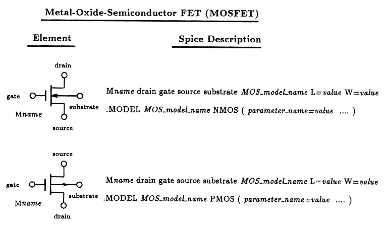
Do not identify source and drain merely from whether they are drawn above or below a symbol. Schematics may be rotated or mirrored. Instead, use the terminal labels, the symbol convention used by the design kit, and the applied voltages.
For a four-terminal MOSFET, the standard SPICE instance ordering is:
For example, an NMOS with drain at out, gate at in, source and body at ground may appear conceptually as:
M1 out in 0 0 nmos_model L=0.5u W=10u
The first node after the name is always the drain, the second is the gate, the third is the source, and the fourth is the body. A swapped drain/source connection may simulate, but it changes the meanings of , , and the body-related voltages. It can also change behavior in a real IC because source and drain are not always perfectly interchangeable once body bias, layout, and process effects are included.
The universal voltage convention
The safest convention is simple:
Read this as “the voltage at terminal , measured with respect to terminal .” The subscript order tells you the subtraction order.
The important MOS terminal voltages are:
You may also encounter:
These are not additional independent voltages. For example,
can be rewritten as
so that
This identity is frequently useful in amplifier analysis.
A voltage label is not an assertion that the answer will be positive. It specifies a reference direction. For instance, if and , then
A negative result is valid information: the gate lies below the source.
Why reference voltages to the source?
The channel is controlled primarily by gate voltage relative to the source, not by gate voltage relative to ground. This is why , rather than , is central to MOSFET analysis.
Similarly, the drain-source voltage
describes the voltage applied along the channel. In later lessons, and will tell us whether a MOSFET is in cutoff, triode, or saturation.
NMOS voltage polarities
In its usual analog-amplifier connection, an NMOS has:
- source at a relatively low voltage,
- drain at a higher voltage,
- gate above the source when the device is on,
- body at the lowest available voltage.
Thus, typical NMOS signs are:
and, when body and source are tied together,
Consider an NMOS with the following terminal voltages:
Then:
Notice that even though the body is at ground, is negative because the source is above ground. Equivalently,
Later, positive for an NMOS will be associated with body effect.
PMOS voltage polarities
A PMOS is the complementary device. In its usual analog connection:
- source is at a relatively high voltage, often near ,
- drain is lower than the source,
- gate must be below the source to turn the device on,
- body is connected to the highest supply voltage.
If we insist on using the same definitions,
and
then a normally conducting PMOS has:
This is completely correct. Negative values do not indicate an error.
For PMOS analysis, it is often more convenient to use source-referenced quantities with positive values:
In normal PMOS operation, these are positive:
Suppose a PMOS has:
Using the universal subtraction convention gives:
Using PMOS-friendly voltage variables gives:
Both descriptions state exactly the same physical voltages. Choose a convention deliberately and retain it throughout the calculation.
Watch “How Does a MOSFET Work?” from Explorer for a visual link between the four terminals, the formation of an NMOS channel, and the distinction between conventional current and electron motion.
Watch the terminal structure first, which identifies source, drain, gate, and body. Then watch channel formation to see why a positive gate-to-source voltage creates an NMOS channel. Finish with current directions; pause there and ensure you can state both the conventional-current direction and the electron-flow direction.
Source and drain: physical symmetry versus circuit labels
A beginner-friendly rule is:
- For an NMOS, the source is normally the terminal at the lower voltage.
- For a PMOS, the source is normally the terminal at the higher voltage.
This rule fits the intended direction of carrier injection:
| Device | Typical source voltage | Typical drain voltage | Carrier motion in channel |
|---|---|---|---|
| NMOS | Lower | Higher | Electrons move from source to drain |
| PMOS | Higher | Lower | Holes move from source to drain |
At the physical level, source and drain diffusion regions are often made similarly, and a simple MOSFET can appear symmetric. But in analog circuit analysis, the designation matters because:
- We define control voltage with respect to the source.
- The body-source junction should remain reverse biased.
- Body effect depends on the source-body voltage.
- Real devices may have layout or process asymmetries.
The source is therefore not just “the lower pin on the drawing.” It is the terminal chosen to serve as the channel’s source under the intended bias condition.
The USC MOS theory notes summarize the practical rule well:
[PDF] Semiconductor Material MOS Theory
Read these short course notes to reinforce the body-bias rule and the practical source/drain labeling rule used in integrated CMOS circuits.
In the pages headed “Body Terminal” and “Conventions,” read the body-bias discussion, focusing on why NMOS bodies are usually tied to ground and PMOS bodies to V_{DD}. Then, on the following “Source or Drain” page, read the source/drain rule. Treat these as normal-bias conventions for analog circuits, not as a substitute for checking every terminal voltage.
Current directions: conventional current is the circuit convention
Circuit equations use conventional current, defined as the direction positive charge would move. Electron motion is opposite to conventional current.
NMOS
For an NMOS in normal operation:
- electrons move from source to drain;
- conventional drain current flows from drain to source.
Thus, we define positive drain current as entering the drain:
This is the current direction used by the usual NMOS drain-current equations.
PMOS
For a PMOS in normal operation:
- holes move from source to drain;
- conventional current also flows from source to drain.
Thus, physical conventional current enters the PMOS source and leaves its drain.
Here is where notation can become confusing. If you keep the universal terminal-current convention “current is positive when entering the named device terminal,” then normal PMOS drain current is negative:
because conventional current is leaving the drain rather than entering it.
For hand calculations, designers commonly avoid carrying this negative sign by defining a positive PMOS current magnitude:
or simply writing as a positive magnitude while explicitly stating that it refers to a PMOS current flowing from source to drain. Both practices occur in textbooks and design discussions.
The key is not which notation you choose. The key is never to mix them silently.
| Quantity | NMOS in normal operation | PMOS in normal operation |
|---|---|---|
| Conventional channel current | Drain to source | Source to drain |
| Electron motion | Source to drain | Drain to source |
| Typical positive voltage notation | , | , |
| Common positive current magnitude | , drain to source | , source to drain |
A universal terminal-current check
When working rigorously, define every terminal current as positive into the transistor:
This is simply KCL applied to the device boundary.
At DC, gate current is ideally negligible:
If the body current is also negligible, then:
For a normally operating NMOS, and . For a normally operating PMOS, and . This single convention works for both device types and is especially useful in simulator outputs, where signs may otherwise be surprising.
A reliable labeling workflow
Whenever you encounter a MOS transistor in a schematic, follow this sequence before writing an equation.
-
Identify device type.
Determine whether it is NMOS or PMOS from the label, PDK symbol, or circuit context. -
Label all terminals.
Mark , , , and . If the body is omitted, state the assumed body connection. -
Write the actual node voltages.
Use values or names such as , ground, , and . -
Construct terminal-voltage differences from their definitions.
For example,rather than relying on visual intuition.
-
State a current reference direction.
For rigorous work, use positive current entering every named terminal. For PMOS magnitude calculations, clearly write whether current is or a magnitude . -
Perform a physical reasonableness check.
A normally on NMOS should generally have a positive ; a normally on PMOS should generally have a positive .
This workflow prevents common errors before any algebra begins.
Common mistakes to eliminate now
Treating as “gate voltage”
is not the gate voltage relative to ground. It is a difference:
If the source moves, changes even when the gate node remains fixed. This fact is the central idea behind the source follower studied later.
Changing the definition for PMOS without saying so
Do not write merely because the device is PMOS. That quantity is named . Preserve the order in the subscript:
Assuming current direction from the arrow alone
MOS symbol-arrow conventions vary among drawing standards and PDKs. Use terminal labels and stated voltage/current references. In exam problems, the indicated current arrow or equation convention is authoritative.
Forgetting the body
Even when no body pin is visible, it is electrically present. An NMOS source raised above its grounded body, or a PMOS source pulled below its -connected body, can experience body effect. We will quantify this later.
Key takeaways
A MOSFET is a four-terminal device with gate , drain , source , and body . In standard integrated CMOS use, the NMOS body is usually tied to the lowest supply and the PMOS body to the highest supply, preserving reverse-biased body junctions.
Use one universal voltage definition:
In particular:
For NMOS devices, normal operation usually gives positive and . For PMOS devices, the same universal definitions normally yield negative and , so designers often use the positive quantities:
Conventional NMOS current normally flows drain to source, while conventional PMOS current normally flows source to drain. Electron motion is opposite to conventional current.
Next, you will use these terminal voltages to determine whether a MOSFET is in cutoff, triode, or saturation—the operating-region classification that determines which current model is valid.
Can't find a good explanation? Sign up and we'll make it for you
Sign up